Scaling optical interconnects for the AI era

Scaling AI demands a new interconnect roadmap, moving from electrical to optical interconnects, and bringing the optics ever closer to the silicon.
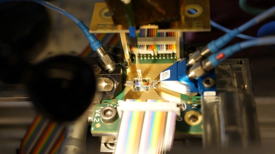 The explosive growth of cloud computing and AI – from generative, and reasoning, to (ultimately) agentic systems – is creating unprecedented demand for bandwidth, as the amount of data that must be moved both within and between data centers continues to surge. In turn, this exposes growing limitations in the underlying interconnects that not only span the data center fabric and rack level but also extend deep inside servers – down to where they link XPUs, memory, and other system components at the package and die level.
Copper-based (electrical) interconnects have long been the industry’s workhorse thanks to their low cost, simplicity, and reliability. Yet today, they are increasingly hitting fundamental limits: while highly energy-efficient electrical links can be realized, they are typically confined to very short reaches (on the order of millimeters). At longer distances and higher lane rates, power consumption rises sharply, thermal constraints intensify, and signal integrity degrades. In other words, electrical I/O is rapidly becoming a key barrier to scaling next-generation AI and machine learning systems.
Optical interconnects have emerged as a critical path forward. By transmitting data using light rather than electrical signals, they are far less sensitive to distance, enabling much better energy efficiency while mitigating many of the crosstalk and thermal challenges inherent to copper links. However, even optical technologies are now being pushed to new extremes – as the need emerges for (multi) terabit-per-second interfaces, ultra-high energy efficiency, and extremely low (sub-microsecond) latency.
Meeting these requirements will take more than incremental innovation. It calls for a fundamental rethinking of the optical interconnect roadmap; one that progressively brings optics closer to the silicon – from the front panel, into the package, and ultimately firmly integrated into the wafer stack.
To read the full article, click here
Related Chiplet
- Optical Chiplet
- Reverse Gearbox Chiplet
- FlexGen Multi-Die Smart Network-on-Chip (NoC) IP
- Ncore Multi-Die Interconnect IP
- Integrated voltage regulator (IVR) chiplet
Related Blogs
- Let’s Get Serious: TeraPHY™ Optical Engine Passes the Test for AI Scale-Up at Volume
- Advancing High‑Performance Silicon Photonics and Silicon Germanium (SiGe) for the Next Era of Optical Connectivity
- Tackling Key HBM and Advanced Packaging Bottlenecks for the AI Era
- 3D IC design for the AI era: an EDA perspective