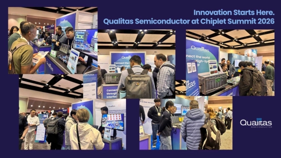
2026 Chiplet Summit: Interconnect is the New Frontier of System Performance
The 2026 Chiplet Summit was far more than a typical technology exhibition. As the market for AI accelerators, data center infrastructure, and High-Performance Computing (HPC) continues to explode, this event served as a definitive confirmation: the bottleneck of system performance has officially shifted from raw computational power to interconnect technology.
In the Era of Chiplets, Interconnect is Competitive Advantage
 Modern semiconductors for AI and data centers have become so complex that the traditional monolithic approach—cramming everything into a single die—has reached its physical and economic limits. Larger chips lead to lower yields, physical reticle size constraints, and exponentially rising costs.
The solution? Chiplets. Instead of one massive chip, multiple smaller, functional dies are manufactured separately and integrated into a single package—much like assembling LEGO blocks.
However, this transition introduces a critical challenge: data movement. If the "highways" (interconnects) between these Chiplets are slow or power-hungry, the entire system’s performance collapses, regardless of how powerful the individual chips are. In the Chiplet era, the ability to connect chips faster and more efficiently is the ultimate differentiator.
This is where Qualitas Semiconductor takes center stage. We have specialized in developing high-speed interconnect IP designed to eliminate speed degradation and power loss. Our core value lies not just in "connecting" chips, but in doing so with industry-leading speed, minimal power consumption, and uncompromising stability.
PCIe Gen 6.0 Live Demo: Bringing Working Silicon to the Booth
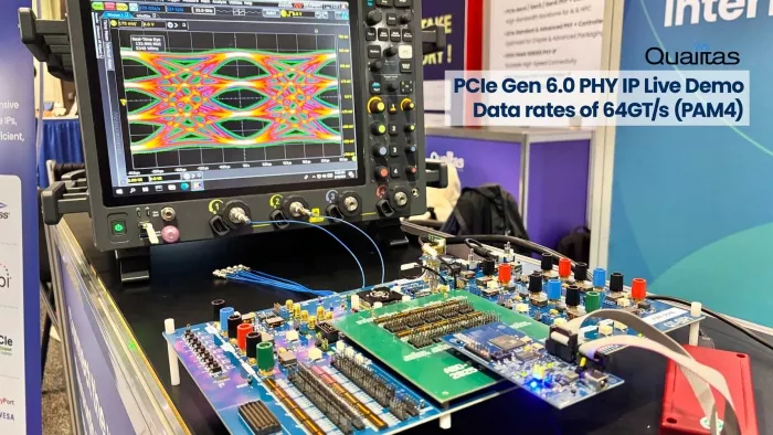
At this year's summit, Qualitas Semiconductor turned heads with a Live Demo of our PCIe Gen 6.0 PHY Test Chip.
Rather than relying on static slides, we brought actual silicon and precision measurement equipment to the floor, proving that our PHY IP is alive and functioning in real-time.
In the semiconductor industry, "working silicon" speaks louder than words. Signal quality in a PHY IP is difficult to guarantee through simulations alone, as it depends on real-world process, package, and board environments. By demonstrating live measurement results, we provided the strongest possible evidence of our technical maturity.
Verifying Signal Quality: The PAM4 Eye Diagram
The oscilloscope at our booth displayed a vivid 64Gbps PAM4 signal. To achieve double the bandwidth of Gen 5.0, PCIe Gen 6.0 transitioned from NRZ (two levels) to PAM4 (four levels). While PAM4 allows for higher data density, the narrower gaps between signal levels make it extremely sensitive to noise.
The "Eye Diagram" is the visual litmus test for signal integrity. A wide, clear "eye" opening indicates high quality. Our demo showcased three distinct, uniform eye layers—a prerequisite for stable operation in complex systems.
Why this matters to our customers: We emphasized the high correlation between our simulation models and actual silicon measurements. For engineers facing tight schedules for AI SoC development, this reliability reduces design risks and can save months of debugging time.
UCIe 2.0: The Real-World Implementation of D2D Interconnect
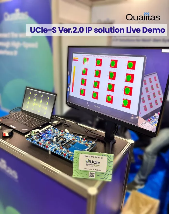
The highlight of our exhibit was the UCIe 2.0-based Die-to-Die (D2D) link Live Demo. UCIe (Universal Chiplet Interconnect Express) is the open standard backed by giants like Intel, TSMC, Samsung, and AMD. It is set to become the "universal language" of the Chiplet ecosystem.
Key features of our UCIe 2.0 demo included:
In-chip Eye Opening Monitor (EOM): We displayed signal margins directly on-screen using internal diagnostics rather than external gear. This is crucial for mass production, where external probing is impossible.
Channel Flexibility: We demonstrated stable "eyes" for both Short-reach (2mm) and Long-reach (25mm) conditions. Whether chiplets are side-by-side or separated on a substrate, our PHY IP adapts seamlessly.
Total Validation: By showing successful Link-up, Far-end Loopback, and Real-time Margin Monitoring simultaneously, we signaled to the market that we are not just "ready on paper"—we are ready for deployment.
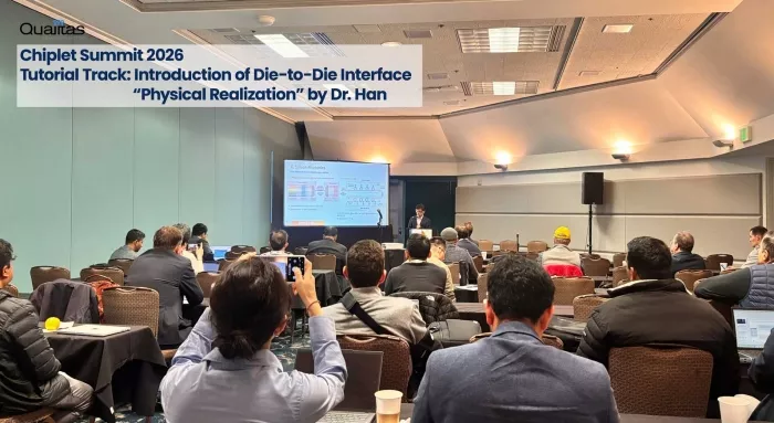
Insights from the Tech Session: "The Physical Realization of Chiplet Systems"
Our CTO, Dr. Pyungsu Han, delivered a tutorial session focusing on the practical hurdles of Chiplet implementation.
Package Interconnect Strategies in Chiplet Design: He discussed the scale gap between nanometer-scale on-chip wiring and millimeter-scale PCB traces. The industry is moving toward Hybrid Bonding (copper-to-copper) to achieve radical connection density, as seen in technologies like TSMC’s CoWoS and Intel’s Foveros.
PDN (Power Delivery Network) in Chiplet packages: In a Chiplet structure, multiple dies share an interposer, making power noise management a nightmare. The solution involves placing MIM/Deep Trench capacitors closer to the Chiplets and moving voltage regulation inside the package.
Silicon Photonics in Chiplets: As electrical signals hit their limits, Silicon Photonics and CPO (Co-Packaged Optics) are emerging. This will be the next chapter for AI clusters that require massive data throughput with high efficiency.
Conclusion: Interconnect is the Heart of Next-Gen Systems
The message from the 2026 Chiplet Summit is clear: Next-generation competitiveness is decided by the interconnect.
With silicon-proven PCIe Gen 6.0 and UCIe 2.0 technologies, Qualitas Semiconductor is moving beyond being a simple IP vendor.
We are becoming an Architecture Partner, working with customers from the earliest design stages to successful Tape-out.
The era of chiplets has arrived, and Qualitas Semiconductor is at the heart of it.
Related Chiplet
- eFPGA Chiplet
- DPIQ Tx PICs
- IMDD Tx PICs
- Near-Packaged Optics (NPO) Chiplet Solution
- High Performance Droplet
Related Blogs
- Addressing the Colossal Challenge of System Co-Optimization with a Holistic Chiplet Design Methodology
- The Chiplet Center of Excellence sets new standards for the automotive industry
- OCP Open Chiplet Economy is Leading the Next Wave of AI: Inference
- Cadence Sets the Gold Standard for UCIe Connectivity at Chiplet Summit '24
Latest Blogs
- How Intel Foundry Packaging Technologies Redefine AI and HPC Scalability Limits at ECTC 2026
- From complexity to simplicity: Scaling and future-proofing chiplets with AMBA®︎ CHI C2C property negotiation
- High-Speed Heterogeneous Integration with Multiphysics Analysis for TSMC SoW-X
- Chiplet Realization Beyond the Package: Why the Next AI Bottleneck Moves to the Interposer-to-PCB Boundary
- Advancing UCIe Performance: Enabling 40G for Next-Generation Multi-Die Designs