AI Memory Is More Than HBM: The Chiplet Era Is Forcing the Entire Memory Hierarchy to Scale

AI systems are usually discussed from the top of the memory hierarchy: on-die SRAM, HBM beside the accelerator, and DDR in the server.
But the hierarchy does not end there.
Training datasets, model checkpoints, inference data, and persistent storage increasingly depend on massive NAND capacity. As AI infrastructure scales, pressure moves downward through the memory hierarchy:
SRAM → HBM → DDR → NAND
Each layer solves a different bandwidth, latency, capacity, and cost problem.
That means AI memory scaling is not only a packaging challenge.
It is also becoming a manufacturing-control challenge.
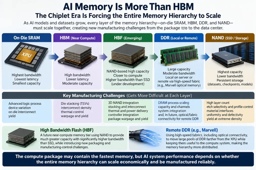
In HBM, the critical issues include die stacking, interconnect density, thermal behavior, warpage, and yield.
In advanced 3D NAND, the challenge shifts toward layer count, etch depth, selectivity, profile control, material interfaces, and uniformity.
And as these structures become taller and denser, manufacturing becomes progressively harder. Small variations in etch profile, film thickness, alignment, interface quality, or process uniformity can propagate across hundreds of layers and directly affect electrical performance and yield.
The connection is important.
AI does not consume one type of memory. It consumes a hierarchy.
And every layer of that hierarchy is becoming harder to manufacture as capacity and bandwidth increase.
A future addition may be High Bandwidth Flash, or HBF. HBF is being developed as a new near-compute tier between HBM and conventional SSD storage, using NAND to provide much greater capacity while moving far closer to accelerator-class bandwidth.
If HBF matures, the hierarchy may evolve toward:
SRAM → HBM → HBF → DDR / SSD
That would not eliminate HBM. It would create another capacity tier for workloads where keeping very large model weights or data sets close to the XPU matters more than DRAM-like latency.
Marvell is pushing a related idea from another direction: using high-speed fabrics, including optical connectivity, to move large pools of DDR farther from the XPU while still keeping them useful to the compute system. That could make the future memory hierarchy more physically distributed, not just more deeply stacked.
But HBF would also introduce another manufacturing challenge.
The closer NAND moves toward the compute package, the tighter the requirements become for stacking, interconnect density, thermal control, power delivery, controller integration, package warpage, and known-good-die yield. A technology designed to close the bandwidth gap could therefore create a new packaging and manufacturing-control problem of its own.
For chiplet architectures, the lesson is broader:
The compute package may contain the fastest memory, but system performance depends on whether the entire memory hierarchy can scale economically.
That makes memory manufacturing part of the AI architecture discussion, even when the NAND itself is not inside the package.
Moh’s Golden Rule:
Do not optimize the fastest memory tier and ignore the capacity tiers feeding it.
AI memory scaling is increasingly a system problem—and a manufacturing problem.
© 2026 Moh Kolbehdari. All rights reserved.
Related Chiplet
- Optical Chiplet
- Reverse Gearbox Chiplet
- FlexGen Multi-Die Smart Network-on-Chip (NoC) IP
- Ncore Multi-Die Interconnect IP
- Integrated voltage regulator (IVR) chiplet
Related Blogs
- UMI: Extending Chiplet Interconnect Standards To Deal With The Memory Wall
- Enabling the Chiplet Era
- Embracing the Chiplet Journey: The Shift to Chiplet-Based Architectures
- Inside the Chiplet Revolution: How Arm’s Compute Subsystems Platform is Democratizing Custom AI Silicon
Latest Blogs
- AI Memory Is More Than HBM: The Chiplet Era Is Forcing the Entire Memory Hierarchy to Scale
- The AI Packaging Challenge: 5 Reasons Panels Are Gaining Momentum
- Understanding the Shift Towards Chiplet Architecture in SoC Design
- Cooling Is Becoming Part of the Chiplet Architecture
- When AI Moves the World: Building a Chiplet Standard for Physical AI