Optical Chiplets Need a Manufacturing Stack, Not Just a Device Roadmap

AI-driven optical connectivity is pulling InP wafers, photonic devices, heterogeneous integration, process control, test, and yield into the chiplet ecosystem.
The first question for optical chiplets was architectural:
Where should electrical communication end and optical communication begin?
The next question is increasingly physical:
How do we manufacture that architecture repeatedly, at useful yield and at AI-infrastructure scale?
That distinction matters.
A photonic integrated circuit can demonstrate excellent bandwidth. An InP laser can deliver the required wavelength and optical power. An electronic IC can successfully drive the optical device. A package architecture can place those functions close to compute.
But none of those accomplishments alone creates a scalable optical-chiplet product.
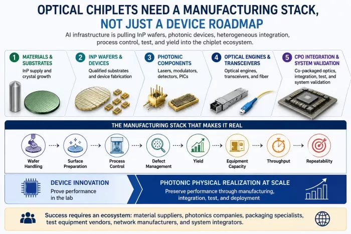
As optical connectivity becomes a larger part of AI infrastructure, the chiplet ecosystem has to absorb an additional manufacturing stack—one that extends from compound-semiconductor wafers and photonic-device fabrication through heterogeneous integration, optical attach, thermal control, test, yield, and qualification.
The optical chiplet is therefore not simply another die added to the package.
It brings another physical realization chain into the chiplet ecosystem.
The Laser Is Part of the Chiplet System
There is an important architectural distinction here.
An InP laser is not necessarily fabricated inside the silicon-photonics chiplet itself.
Depending on the architecture, the light source may be external, separately packaged, heterogeneously integrated near the PIC, bonded onto another structure, or implemented as a distinct optical chiplet.
That means a future optical-chiplet system may contain several technology domains:
compute/SerDes silicon → EIC → PIC → InP laser source → optical coupling → fiber
The dies may originate from completely different semiconductor processes.
The compute device may use an advanced CMOS node.
The electronic interface IC may use another optimized CMOS process.
The PIC may use silicon photonics.
The laser may come from an InP process.
Then packaging has to turn those individually optimized technologies into one functioning optical system.
That is where the manufacturing problem becomes fundamentally heterogeneous.
Why InP Matters
Indium phosphide, or InP, is particularly important because of its ability to efficiently generate light at wavelengths widely used in optical communications.
Silicon is extraordinarily capable for logic and can support many passive and active photonic functions, but it is not an efficient native light emitter because of its indirect bandgap.
InP is different.
Its direct-bandgap characteristics make it well suited for lasers and other active photonic devices used in high-speed optical communication.
But those material advantages come with a different manufacturing environment.
Mainstream silicon manufacturing has spent decades developing large, highly automated wafer-processing infrastructure around 300-mm wafers.
InP manufacturing generally operates with smaller substrates, more fragile material, different process requirements, and a less mature high-volume manufacturing ecosystem.
That difference becomes increasingly important as AI pushes optical connectivity toward larger deployment volumes.
The Manufacturing Stack Is Starting to Move
A recent example comes from Applied Optoelectronics, Inc. (AOI), which grows and fabricates InP laser devices for optical transceivers used in data-center connectivity.
Trymax recently announced a multi-year equipment agreement with AOI supporting expansion of that InP laser-chip production.
The equipment itself—plasma ashers and UV-based surface-processing systems—may sound far removed from the architectural discussions around optical I/O and co-packaged optics.
It is not.
It is evidence that demand is beginning to propagate upstream into the manufacturing equipment required to produce photonic devices repeatedly.
As volume increases, the engineering problem expands into:
wafer handling → surface preparation → process control → defect management → yield → equipment capacity → throughput → manufacturing repeatability
That is a very different problem from demonstrating that an InP laser works.
Capacity and Repeatability Are Not the Same Thing
AI optical scaling is already generating discussion around InP wafer capacity, laser capacity, silicon-photonics capacity, fiber availability, and optical-transceiver production.
Those questions are important.
But manufacturing capacity alone does not guarantee product capacity.
A fab can have wafer starts available.
A supplier can have laser designs.
An assembly line can have nominal capacity.
Yet the resulting optical system may still be difficult to scale if device performance varies too much, optical alignment windows are too narrow, package stress changes optical behavior, test time becomes excessive, or yield deteriorates as integration complexity increases.
This is the distinction between capacity and repeatability.
Capacity answers:
How many can we attempt to build?
Repeatability answers:
How many can we build while preserving the required performance and margin?
For optical chiplets, the second question may ultimately be more important.
The Chiplet Manufacturing Boundary Expands
Traditional chiplet manufacturing already has to coordinate known-good-die strategy, bumping, interposers, RDL, substrates, underfill, warpage, thermal solutions, electrical test, assembly sequence, and yield.
Photonics adds another set of tightly coupled variables.
Optical alignment must survive assembly.
Laser performance must remain stable across operating temperature.
Mechanical movement can alter coupling.
Fiber attach must be manufacturable.
Electrical and optical test must be correlated.
Different dies may have different thermal limits and known-good-die requirements.
Repair and rework become more complicated.
And every additional heterogeneous interface creates another opportunity for yield loss.
The chiplet problem therefore evolves from:
Can these dies communicate?
to:
Can these dies be manufactured, integrated, tested, and qualified together with repeatable system performance?
This is where optical chiplets become a manufacturing architecture, not simply a connectivity architecture.
Device Performance Has to Survive the Journey
A useful way to think about optical-chiplet maturity is to follow capability across the physical chain:
device capability → wafer fabrication → die integration → package environment → manufacturing variation → test → qualified system
The objective is not merely to preserve connectivity.
It is to preserve the physical conditions that made the device valuable in the first place.
A laser can have excellent output power and spectral characteristics.
A modulator can demonstrate exceptional bandwidth and efficiency.
A PIC can deliver low optical loss.
But if those advantages disappear after thermal loading, stress, alignment variation, assembly, or process variation, the device achievement has not yet become a system advantage.
That is why the next optical-chiplet race may increasingly move away from headline device metrics alone.
Bandwidth and energy per bit will remain critical.
But process window, wafer throughput, test coverage, assembly tolerance, yield, reliability, and manufacturing stability will become equally important measures of maturity.
From Optical Chiplet to Optical-Chiplet Ecosystem
The chiplet ecosystem becomes powerful when different companies can provide different pieces while the overall system remains integratable.
Optical chiplets expand that ecosystem upstream and downstream.
The supply chain now potentially includes compound-semiconductor substrate suppliers, InP fabs, silicon-photonics foundries, electronic-IC suppliers, laser vendors, optical-engine companies, advanced-packaging providers, OSATs, fiber-attach specialists, process-equipment suppliers, test-equipment companies, and system integrators.
The opportunity is enormous.
But it also means that no single photonic breakthrough is sufficient.
An optical chiplet is only as scalable as the manufacturing chain that surrounds it.
The Next Optical-Chiplet Question
The first optical-chiplet question was:
Where should the E/O boundary move?
The next one is:
Can the manufacturing ecosystem preserve the required optical capability as that boundary moves into increasingly heterogeneous packages?
That question reaches from the InP wafer all the way to the AI system.
And it may become one of the defining challenges of the next phase of chiplet adoption.
The photonic chiplet is not only a new device in the package. It pulls a new manufacturing ecosystem into the chiplet supply chain.
The next optical-chiplet race will therefore not be won only by the best laser, modulator, or PIC.
It will be won by the architecture and manufacturing ecosystem that can turn those devices into a repeatable, testable, qualified heterogeneous system at scale.
© 2026 Moh Kolbehdari. Original technical perspective. All rights reserved.
Related Chiplet
- FlexGen Multi-Die Smart Network-on-Chip (NoC) IP
- Ncore Multi-Die Interconnect IP
- Integrated voltage regulator (IVR) chiplet
- High-performance connectivity chiplets
- eFPGA Chiplet
Related Blogs
- What are Chiplets? - The Key Technology Behind Next-Gen Semiconductor Manufacturing
- The Next Chiplet Era: Compute Meets Optical Chiplets
- What are chiplets?
- RISC-V Chiplets, Disaggregated Die, and Tiles
Latest Blogs
- Chiplet Modularity Is Becoming Part of the AI Architecture
- Hierarchies Of Interconnects Are As Important As Compute And Memory
- UALink over UCIe 3.0: Maximizing Performance for Chiplet-based Designs
- Physical AI Doesn't Just Scale Up. It Scales Out.
- Ayar Labs and GUC Complete Successful Thermal Co-Simulation Testing of Co-Packaged Optics