Cooling Is Becoming Part of the Chiplet Architecture

Chiplet architectures are usually described in terms of compute, memory, I/O, interconnect, and increasingly optics.
But another element is moving closer to the architectural boundary.
Cooling.
For earlier generations of semiconductor products, the thermal solution could often be treated largely as something attached after the package architecture had already been defined. The package generated heat. The cooling system removed it.
That separation is becoming harder to maintain.
AI and HPC packages are becoming larger, more heterogeneous, and more power-dense. Compute chiplets may sit beside HBM stacks, I/O die, optical engines, bridges, interposers, and multiple package interfaces. Each element can have a different power density, temperature profile, mechanical behavior, and sensitivity to deformation.
The result is that the cooling system does more than remove heat.
It helps establish the physical environment in which the chiplet system operates.
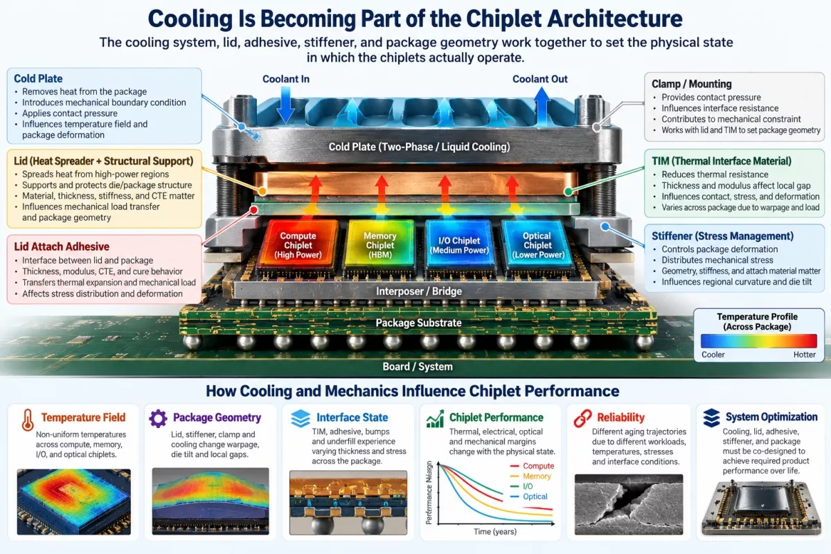
Cooling Changes More Than Temperature
Consider a cold plate attached to a large AI package.
Its obvious function is thermal.
But physically, the cold plate also introduces contact pressure, mechanical constraint, interface loading, and a temperature field that may vary significantly across the package.
Those conditions interact with the lid, TIM, stiffener, substrate, die, HBM, interposer, and board.
A useful physical sequence is:
Cooling / Lid / Stiffener / Clamp → Temperature & Structural Constraint → Warpage / Stress / BLT / Alignment → Product Behavior
This matters because package geometry does not remain fixed after design.
A cold plate changes the temperature field.
The temperature field changes material response.
Material response changes stress and deformation.
Deformation can change TIM bond-line thickness, coplanarity, die tilt, local contact pressure, optical alignment, bump stand-off, and interface stress.
Those changes can then appear as thermal, mechanical, electrical, or optical performance differences.
So the thermal solution becomes part of the package realization problem.
The Lid Is More Than a Heat Spreader
The lid serves both a structural and a thermal role.
Thermally, it helps spread heat from concentrated die regions toward the cooling solution.
Mechanically, it helps protect and support the die/package structure while influencing how loads and deformation are transferred across the package.
Its material, thickness, stiffness, CTE, geometry, and attach condition therefore matter at the system level.
The lid attach adhesive is part of that behavior as well.
Its thickness, modulus, CTE, adhesion, and cure behavior influence how thermal expansion, mechanical load, and deformation are transferred between the lid and package.
A lid that improves heat spreading can still alter package curvature.
A different stiffness can redistribute stress.
CTE mismatch can change deformation during thermal excursions.
And the adhesive layer can either accommodate or transmit part of that movement.
The lid therefore should not be treated as only a thermal component.
It is part of the thermal-mechanical architecture of the package.
The best lid solution is not necessarily the material with the highest thermal conductivity.
It is the solution that provides the right combination of heat spreading, structural support, stiffness, CTE behavior, interface stability, package geometry, and reliability.
Stiffeners Are Stress-Management Elements
A stiffener is primarily a mechanical element.
Its role is not simply to make the package “stronger.”
Its geometry, stiffness, attach material, and placement influence how stress is distributed and how deformation develops across the substrate.
That becomes especially important in large heterogeneous packages containing compute chiplets, HBM, I/O die, optical engines, and regions with very different thermal and mechanical behavior.
A stiffener can reduce deformation in one region while changing the stress state elsewhere.
That is why stiffener design is fundamentally about stress distribution and deformation control.
A useful sequence is:
Stiffener Geometry / Attach → Stress Distribution → Regional Deformation → Local Interface State → Product Behavior
This also makes the distinctions cleaner:
Lid → structural support + heat spreading
Lid adhesive → load transfer + thermal-mechanical coupling
Stiffener → stress distribution + deformation control
Clamp → applied load / contact pressure
TIM → thermal interface + geometry/contact sensitivity
Cold plate → cooling + mechanical boundary condition
Chiplet Systems Make the Problem More Complicated
A monolithic die already presents a difficult thermal-mechanical problem.
Chiplet systems add asymmetry.
Different chiplets can have different sizes, thicknesses, workloads, power densities, bump structures, thermal paths, and interface requirements.
The package itself may contain regions with very different stiffness and thermal response.
Consider a heterogeneous AI package containing compute chiplets and HBM.
The compute region may generate the highest heat flux.
The HBM region may have different package height and thermal sensitivity.
An I/O die may operate at lower power but depend on stable electrical geometry.
An optical engine may have comparatively modest power while being highly sensitive to alignment.
Now add the lid, TIM, stiffener, clamp, cold plate, board, and cooling distribution.
The question is no longer simply whether the package stays below a junction-temperature limit.
The question becomes:
What physical state does the entire package assume under the actual thermal and mechanical environment of the product?
Local, Regional, and Global Effects Become Connected
This is where chiplet architecture and physical realization begin to converge.
A package can experience effects at several spatial scales simultaneously.
A local TIM thickness variation may alter the thermal path beneath one die.
Regional package curvature may create tilt across an HBM or optical-engine region.
Global package bow may change coplanarity or the overall mechanical interaction with the board and cooling structure.
These effects can propagate.
A global constraint can produce regional deformation.
Regional deformation can create a local interface shift.
The local change can then become a product-level thermal, electrical, mechanical, or optical consequence.
The reverse can also occur.
A local interface condition, such as underfill shrinkage or TIM contact variation, can redistribute stress regionally and contribute to larger package deformation.
This means that chiplet integration cannot always be partitioned neatly into independent thermal, mechanical, electrical, and optical problems.
The physical package connects them.
The Physical Environment Becomes Part of Architecture
This leads to a larger architectural implication.
Chiplet architects traditionally decide where functions belong.
Compute here.
Memory there.
I/O somewhere else.
Optics near the package edge.
Those decisions are still fundamental.
But future chiplet architecture may increasingly need to consider where those functions sit relative to the thermal and mechanical environment of the package.
- Where is the highest heat flux?
- Where is the stiffest region?
- Where will the lid or cold plate impose the strongest constraint?
- Where will temperature gradients be largest?
- Which chiplets are most sensitive to tilt?
- Which interfaces are most sensitive to BLT?
- Where does optical alignment have to remain stable?
These questions connect functional partitioning to physical realization.
Cooling therefore becomes more than infrastructure.
It becomes part of architectural placement and package geometry.
From Thermal Design to Physical-State Design
The shift can be summarized simply.
Traditional thermal design asks:
Can the cooling solution remove enough heat?
The emerging problem asks:
What physical state does the cooling solution create while removing that heat?
That difference is important.
A cooling system can meet the thermal target while still creating undesirable package deformation, local TIM variation, excessive clamp loading, optical alignment shift, or long-term interface stress.
The full engineering chain is therefore closer to:
Cooling Architecture → Temperature Field + Structural Constraint → Package Geometry → Interface State → Chiplet Performance
This is especially important for heterogeneous systems because different chiplets do not necessarily have the same tolerance to the same package movement.
The Package Is Becoming Part of the Cooling System — and the Cooling System Part of the Package
As AI systems scale, the boundaries between chip, package, cooling, power delivery, optics, and system integration are becoming less distinct.
That does not mean every discipline becomes one discipline.
It means their physical interfaces increasingly determine system behavior.
For chiplet systems, cooling can no longer be treated only as a downstream system problem.
- The cold plate matters.
- The lid matters.
- The stiffener matters.
- The clamp matters.
- The TIM matters.
- The board matters.
And the interaction among them helps determine the physical geometry in which the chiplets actually operate.
The next generation of chiplet architecture will therefore require more than functional partitioning.
It will require physical-state awareness.
Because the question is no longer only where the chiplets are placed.
It is also:
What physical environment are we placing them into?
© 2026 Moh Kolbehdari. All rights reserved.
Related Chiplet
- Optical Chiplet
- Reverse Gearbox Chiplet
- FlexGen Multi-Die Smart Network-on-Chip (NoC) IP
- Ncore Multi-Die Interconnect IP
- Integrated voltage regulator (IVR) chiplet
Related Blogs
- Chiplet Modularity Is Becoming Part of the AI Architecture
- OCP Open Chiplet Economy is Leading the Next Wave of AI: Inference
- 2026 Chiplet Summit: Interconnect is the New Frontier of System Performance
- The Chiplet Consolidation Wave: How Strategic Acquisitions are Shaping the Future of Silicon
Latest Blogs
- Cooling Is Becoming Part of the Chiplet Architecture
- When AI Moves the World: Building a Chiplet Standard for Physical AI
- Co-Packaged Optics Moves from Promise to Production Planning
- Co-Packaged Optics Moves from Promise to Production Planning
- Co-Packaged Optics Moves from Promise to Production Planning