3D Chips: Socionext Achieves Two Successful Tape-Outs in Just Seven Months
In the race to deliver high-performance, power-efficient chips — especially 3D multi-die designs for AI and high-performance computing (HPC) applications — speed of design and development is critical.
Setting new benchmarks for complexity and speed, Socionext recently achieved two successful tape-outs for a cutting-edge 3DIC chip in just seven months following initial design kickoff. Based on advanced TSMC-SoIC technology, the chip stacks two heterogeneous dies (compute on TSMC N3 and I/O on TSMC N5) in a face-to-face (F2F) configuration.
To accelerate its workflows and overcome significant technical hurdles, Socionext used a full suite of Synopsys IP, electronic design automation (EDA), and cloud solutions.
“You need the very best partners and solutions to deliver 3D multi-die designs in record speed,” said Rajinder Cheema, CTO and executive vice president at Socionext. “Our collaboration with Synopsys and use of their 3D-enabled IP, AI-powered EDA flows, and cloud solutions helped us overcome significant design complexity, achieve multiple tape-outs in just seven months, and set new standards for innovation and time-to-market.”
|
About TSMC-SoIC® TSMC-SoIC® advances heterogeneous chiplet integration to reduce size and increase performance. TSMC-SoIC® features ultra-high-density vertical stacking that delivers high performance, low power, and minimum resistance, inductance, and capacitance (RLC). |
Synopsys solutions: the engine behind fast, reliable tape-outs
As the complexity of multi-die designs continues to grow, so too does the need for robust, comprehensive design and verification solutions. Our portfolio of best-in-class IP, powerful EDA tools, and scalable cloud resources helped Socionext accelerate every phase of development.
IP solutions
Our extensive portfolio of silicon-proven IP enabled Socionext to integrate key functionality quickly and reliably. By leveraging pre-validated building blocks, their design team was able to focus on differentiation and innovation, rather than reinventing the wheel for foundational components.
- Socionext used our 3D-enabled IP — including 3DIO, PCIe 6.0, DDR5, Test, and SLM Process, Voltage, and Temperature (PVT) monitor — to ensure their design adheres to TSMC SoIC requirements.
- Customized for F2F configuration, our PCIe 6.0 and DDR5 IP allowed Socionext to integrate heterogeneous logic, memory, and interface components in a single package while meeting performance, power, and density targets.
- Our 3DIO IP provided 3D die-to-die connectivity and seamless integration with the Synopsys place and route flow.
EDA tools
Socionext leveraged our advanced EDA tools — from architecture exploration and RTL design to physical implementation and signoff — for the tape-outs. These tools are engineered to handle the unique challenges of multi-die and 3DIC architectures, including complex interconnects, power management, and timing closure. Socionext used:
- Fusion Compiler, which offers AI-driven adaptive flows, to automate chiplet design from RTL to GDSII.
- 3DIC Compiler for co-design of the dies and advanced package — from exploration to signoff.
- Ansys — now part of Synopsys — Redhawk-SC for multiphysics analysis with early-stage thermal and infrared (IR) optimization.
- TestMAX DFT for implementation and timely access to test data, with support for the IEEE 1838 standard.
Cloud EDA environment
Verifying intricate 3DIC designs requires significant computational resources. Socionext leveraged the Synopsys Cloud FlexEDA SaaS environment, giving their designers 2,000 on-demand compute cores and multiple terabytes of storage. The cloud-based approach enabled multiple simulations and analyses to be processed concurrently, reduced bottlenecks, and enhanced technical collaboration across teams and geographies — all of which significantly accelerated design closure.
- Following initial exploration, Socionext used Synopsys Cloud FlexEDA services for the implementation of their 3DIC design.
- The ability to scale resources ensured Socionext could meet tight deadlines and allowed for immediate adjustments in response to design challenges.
- Cloud-based resources enabled closer collaboration and higher productivity across Socionext’s architecture, design, and signoff teams.

Use cases: compact, efficient, and powerful
The Socionext 3DIC chip is poised to make an impact across a range of applications. Its high-performance capabilities and power efficiency make it ideal for AI and HPC workloads, which require massive computational throughput and efficient data handling — often within thermally constrained environments.
Thanks to the advanced integration techniques enabled by TSMC’s SoIC technology and the design optimizations facilitated by our solutions, Socionext’s 3DIC chip delivers the speed and efficiency needed for next-generation neural networks, data analytics, and scientific computing.
The advanced chip also holds promise in the consumer space. From smartphones and wearables to smart home technologies, compact and power-efficient devices are in high demand. The ability to stack dies and optimize them for both size and power consumption means customers can deliver feature-rich products without compromising battery life or form factor.
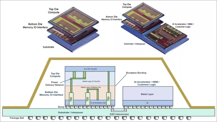
Socionext’s 3DIC F2F and 5.5D structure (Source: Socionext)
Accelerating 3DIC and multi-die innovation
Socionext’s 3DIC tape-out is more than just a technical milestone — it’s a glimpse into the future of semiconductor design.
As traditional scaling approaches reach their physical limits, multi-die designs — where multiple chiplets are combined in a single package — are emerging as a key strategy for continued innovation. This shift brings new challenges, including complex interconnects, heterogeneous integration, and the need for end-to-end design and verification flows.
As the industry continues to push the boundaries of what’s possible, we remain committed to empowering our customers with the IP, EDA, and cloud solutions they need to succeed. Whether it’s enabling faster development cycles, supporting advanced packaging, or assisting new levels of integration and performance, our mission is to help innovators like Socionext bring groundbreaking products to market — quickly and reliably.
Related Chiplet
- eFPGA Chiplet
- DPIQ Tx PICs
- IMDD Tx PICs
- Near-Packaged Optics (NPO) Chiplet Solution
- High Performance Droplet
Related Blogs
- 2024 Forecast: Hybrid Bonding Steps Up
- 3D IC Design Ecosystem Panel at #61DAC
- How 40G UCIe IP Powers Data Center AI Chips
- Advancing 3D IC Design for AI Innovation
Latest Blogs
- How Intel Foundry Packaging Technologies Redefine AI and HPC Scalability Limits at ECTC 2026
- From complexity to simplicity: Scaling and future-proofing chiplets with AMBA®︎ CHI C2C property negotiation
- High-Speed Heterogeneous Integration with Multiphysics Analysis for TSMC SoW-X
- Chiplet Realization Beyond the Package: Why the Next AI Bottleneck Moves to the Interposer-to-PCB Boundary
- Advancing UCIe Performance: Enabling 40G for Next-Generation Multi-Die Designs