Six critical trends reshaping 3D IC design in 2026 and beyond
March 3, 2026

AI compute is scaling at ~1.35× per year, nearly twice the pace of transistor scaling. Thus, the semiconductor industry has reached a hard inflection point: if we can’t scale down, we must scale up. Increasingly, engineering teams are turning to 3D ICs to keep pace with the ascent of next-gen AI scaling.
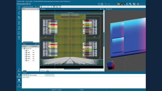 However, designing in three-dimensions also exacerbates system complexity, leaving IC and package designers with a pressing question: how do you explore millions of design considerations and still optimize and validate system performance within schedule constraints?
This article examines six trends that will help design teams overcome this challenge and help them reshape the future of 3D IC design in 2026.
To read the full article, click here
Related Chiplet
- Optical Chiplet
- Reverse Gearbox Chiplet
- FlexGen Multi-Die Smart Network-on-Chip (NoC) IP
- Ncore Multi-Die Interconnect IP
- Integrated voltage regulator (IVR) chiplet
Related Blogs
- Six critical trends reshaping 3D IC design in 2026
- Signal integrity and power integrity analysis in 3D IC design
- Advancing 3D IC Design for AI Innovation
- Maximizing 3DIC Design Productivity with 3DBlox: A Look at TSMC’s Progress and Innovations in 2024