Accelerating Chiplet Innovation with a New Partner Ecosystem

The semiconductor industry is currently undergoing a massive shift. As we push the boundaries of performance in physical AI, data centers, and high-performance computing (HPC), traditional monolithic chip design is hitting physical and economic walls. The answer for many engineers and architects is chiplets, a modular approach that enables the mixing and matching of silicon dies to create powerful, highly customized systems.
 However, transitioning from a single-die SoC (system on chip) to a multi-die SiP (system in package) brings a surge in engineering complexity. How do you ensure different pieces of silicon from different vendors communicate with each other correctly?
To tackle these challenges head-on, Cadence has announced a major leap forward: a Chiplet Spec-to-Packaged Parts ecosystem. This initiative is designed to streamline the engineering process and accelerate time to market. Through our partnerships Cadence is paving a lower-risk path for the next generation of chiplet adoption.
The Spec-to-Packaged Parts Vision
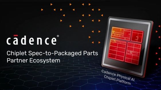
The core of this announcement is the Cadence Physical AI chiplet platform. This isn't just a set of tools. It's a comprehensive configurable platform designed to bridge the gap between a chiplet specification and a final, known-good die (KGD) or packaged (multiple dies) part.
Cadence has built spec-driven automation that generates chiplet framework architectures. These frameworks combine Cadence's own IP with third-party partner IP, all wrapped in critical chiplet management services, as well as built-in security and safety features.
The goal is clear: Accelerate the spec-to-parts process while reducing risk!
Developing chiplets often feels like venturing into uncharted territory. By providing a pre-verified platform, Cadence enables design teams to start with a robust foundation rather than building everything from scratch. In addition to significantly reducing customer-specific chiplet development time, this approach optimizes costs, provides the flexibility needed for customization, and enables configurability that modern applications demand.
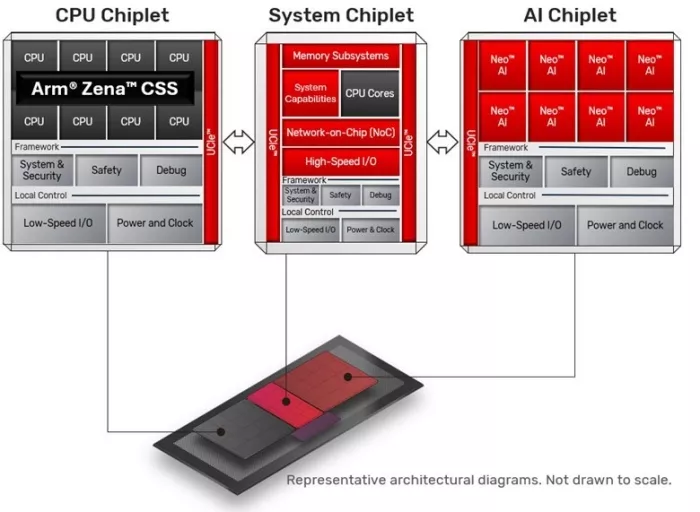
Figure 1. Cadence Physical AI Chiplet Platform
Critically, the generated chiplet architectures are standards-compliant. They adhere to the Arm Chiplet System Architecture and the future OCP Foundational Chiplet System Architecture, ensuring broad interoperability. The Cadence Chiplet Framework encapsulates these capabilities, which are reusable across chiplets, accelerating chiplet development and ensuring cross-chiplet interoperability through standardization.
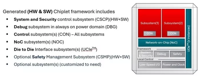
Figure 2. Cadence Chiplet Framework
Strategic Partners: Arm and Samsung
Two key collaborations anchor this new ecosystem, signaling the industry-wide support for this initiative.
Arm: Powering Physical AI
Building on a long history of collaboration, Cadence and Arm have forged a new strategic partnership focused on physical AI.
This agreement grants Cadence access to the advanced Arm Zena Compute Subsystem (CSS). This is a game-changer for edge AI processing requirements in automobiles, robotics, and drones. By integrating Arm's technology, the platform empowers safer, smarter, and more efficient systems.
Samsung Foundry: Future Prototype Silicon Proof
One of the biggest hurdles in chiplet adoption is proving real-world functionality. To showcase Cadence's chiplet expertise and Samsung's semiconductor technology, Cadence is partnering with Samsung Foundry to build a real-world silicon prototype of the Physical AI Chiplet Platform. Using Samsung's SF5A process for automotive, the prototype will feature an Arm Zena CSS-based chiplet, a central system chiplet, and an AI chiplet powered by Cadence Neo NPUs.
A Robust IP Partner and Silicon Analytics Ecosystem
An ecosystem is defined by the strength of its community. Beyond Samsung and Arm, Cadence has enlisted a diverse group of initial IP partners and a silicon analytics company to ensure important aspects of chiplet designs for Physical AI are covered.
- Arteris: Providing physically-aware network-on-chip (NoC) IP products like Ncore for coherent systems and FlexGen for non-coherent ones to handle high bandwidth, low latency, and power-efficient interconnects in multi-die systems.
- eMemory: Contributing enhanced one-time programmable (OTP) memory that complements Cadence's security subsystems, ensuring secure storage and key management.
- M31 Technology: Delivering MIPI PHY interface IP, essential for automotive and high-volume consumer applications requiring flexible camera and display integration.
- proteanTecs: Embedding a hardware health and performance monitoring system for telemetry and silicon analytics SW, per chiplet die and across chiplet types, to enable power-efficient, safe, and reliable performance of next-gen systems.
- Silicon Creations: Providing ultra-fast, multiphase PLL clocking solutions optimized for the Cadence Chiplet Framework, UCIe die-to-die IP, and interface IP.
- Trilinear Technologies: Delivering advanced DisplayPort IP to drive high-performance video connectivity.
Conclusion
As David Glasco, vice president of the Compute Solutions Group at Cadence, noted in our recent announcement, this ecosystem represents a "significant milestone in chiplet enablement."
In an era of skyrocketing design complexity, achieving the necessary performance and cost efficiency demands collaboration and standardization. By combining extensive internal expertise with a powerful network of partners like Arm and Samsung Foundry and specialized IP and silicon analytics providers, Cadence is building a launchpad for the next generation of physical AI and HPC innovations.
For engineers and architects, this means less time wrestling with integration headaches and more time focusing on differentiation and innovation.
Related Chiplet
- eFPGA Chiplet
- DPIQ Tx PICs
- IMDD Tx PICs
- Near-Packaged Optics (NPO) Chiplet Solution
- High Performance Droplet
Related Blogs
- Accelerating Early-Stage explorations with Virtual Prototyping for a thriving multi-vendor chiplet ecosystem
- Accelerating an Open Chiplet Ecosystem for Automotive with Foundation Chiplet System Architecture
- Podcast: How Achronix is Enabling Multi-Die Design and a Chiplet Ecosystem with Nick Ilyadis
- The Growing Chiplet Ecosystem: Collaboration, Innovation, and the Next Wave of UCIe Adoption
Latest Blogs
- How Intel Foundry Packaging Technologies Redefine AI and HPC Scalability Limits at ECTC 2026
- From complexity to simplicity: Scaling and future-proofing chiplets with AMBA®︎ CHI C2C property negotiation
- High-Speed Heterogeneous Integration with Multiphysics Analysis for TSMC SoW-X
- Chiplet Realization Beyond the Package: Why the Next AI Bottleneck Moves to the Interposer-to-PCB Boundary
- Advancing UCIe Performance: Enabling 40G for Next-Generation Multi-Die Designs