Nvidia, TSMC, and advanced packaging realignment in 2025
By Majeed Ahmad, EDN (January 20, 2025)
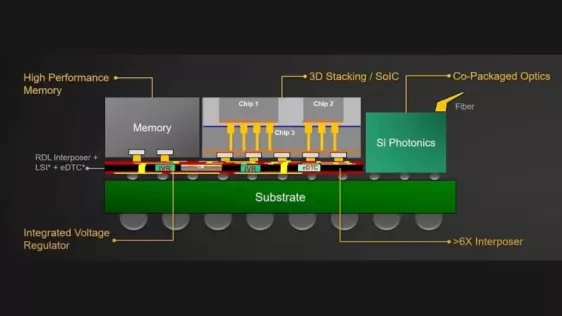
Nvidia’s CEO Jensen Huang has made waves by saying that his company’s most advanced artificial intelligence (AI) chip, Blackwell, will transition from CowoS-S to CoWoS-L advanced packaging technology. That also shows how TSMC’s advanced packaging technology—chip on wafer on substrate (CoWoS)—is evolving to overcome interconnect battles inside large, powerful chips for AI and other high-performance computing (HPC) applications.
The CoWoS-S advanced packaging technology uses a single silicon interposer and through-silicon vias (TSVs) to facilitate the direct transmission of high-speed electrical signals between the die and the substrate. However, single silicon interposers often confront yield issues.
To read the full article, click here
Related Chiplet
- DPIQ Tx PICs
- IMDD Tx PICs
- Near-Packaged Optics (NPO) Chiplet Solution
- High Performance Droplet
- Interconnect Chiplet
Related News
- After TSMC fab in Japan, advanced packaging facility is next
- Amkor and TSMC to Expand Partnership and Collaborate on Advanced Packaging in Arizona
- Lorentz Solution Jointly Presents with NVIDIA on Large-Scale 3D Terahertz EM Simulation for Real IC/3DIC Silicon Case Studies in Photonic Switches at 2025 TSMC OIP
- NVIDIA Reportedly Overwhelms TSMC with 3 and 4-Nanometer Orders
Latest News
- Avicena Launches the World’s First microLED Optical Interconnect Evaluation Kit for AI Infrastructure Innovators
- Lightmatter Achieves Record 1.6 Tbps Per Fiber to Accelerate AI Optical Interconnect
- Arm Positions Neoverse for AI and Telco Networks at MWC
- NVIDIA Compute Architecture Paves the Way for Scale-Up Optical Interconnects; CPO Penetration in AI Data Centers Expected to Rise Steadily
- CEA-Leti and NcodiN Partner to Industrialize 300 mm Silicon Photonics for Bandwidth-Hungry AI Interconnects