Glass Core Substrates and Interposers for Advanced Packaging: Insights from the Intellectual Property Landscape
SOPHIA ANTIPOLIS, France – January 10, 2025 -- Advanced semiconductor packaging is a rapidly evolving field where multiple technologies are being developed simultaneously. The integration of glass into substrates and interposers within semiconductor packages has the potential to accelerate the development of emerging technologies targeting applications such as artificial intelligence (AI), high-performance computing (HPC) and next-generation photonics-based computing.
Rising patent activity and competition within the semiconductor industry
Glass, as a packaging material, offers significant advantages over organic core substrates and silicon interposers. Its stiffness minimizes warpage when multiple chips are integrated, ensuring improved reliability and performance. Additionally, the transparency of glass enables new possibilities for co-packaging photonic and electronic components, paving the way for innovative devices integrating photonic integrated circuits (PIC) and electronic integrated circuits (EIC). This dual functionality positions glass a potentially game-changing material in advanced semiconductor packaging.
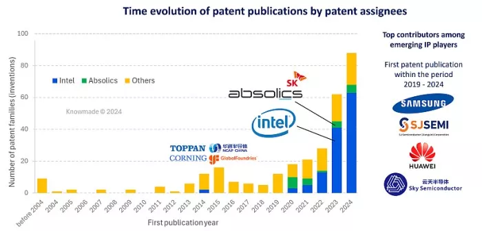
Patenting activities related to glass core substrates and interposers for advanced semiconductor packaging are relatively recent and accelerating (Figure 1). Before 2020, no clear intellectual property (IP) leaders had emerged, although patent filings began increasing around 2015 from players such as Toppan, Corning, NCAP, and GlobalFoundries. Since 2020, the landscape has shifted, with Intel emerging as the leading patent assignee, currently holding nearly half of the patents in this field.

Figure 1: Time evolution of patent publications related to glass core substrates and glass interposers for advanced semiconductor packaging.
Intel stands out for its prolific patenting activity, showcasing a well-balanced patent portfolio that encompasses both glass core substrates and glass interposers, reflecting its strategic commitment to the field. Absolics, a subsidiary of SK Group, is the closest IP competitor, with a patent portfolio focused on glass core substrates. The remaining half of the patent corpus is highly fragmented, with over 150 patent applications filed by approximately 70 companies, each holding only a relatively small number of patents. This diversity highlights the various approaches being pursued to drive innovation in the field. Notably, an increasing number of companies have entered the IP race in recent years, including Samsung, and Chinese firms such as SJ Semi, Xiamen Sky Semiconductor, and Huawei, reflecting the growing industry interest in glass-based packaging.
Patent insights into the innovations shaping the potential adoption of glass in the semiconductor packaging industry
Predominant categories of inventions by top patent applicants
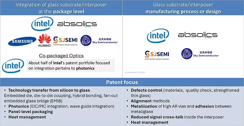
The analysis of patent applications reveals two main categories of inventions involving glass for advanced semiconductor packaging: those where the glass substrate or interposer is integrated at the package level, and those where the glass substrate or interposer itself is engineered through improved manufacturing processes (Figure 2).
In the first category, glass is integrated with other package components and materials, showcasing its robustness and versatility in applications such as cost-effective panel-level packaging and photonics. These applications, including co-integration of EIC and PIC, as well as waveguide integration, benefit from glass’s transparency. Patent portfolios also show a strong emphasis on transferring technologies developed for silicon to glass. Innovations include embedding dies in glass for thinner packages, hybrid bonding of chips to through-glass vias (TGV), and using embedded glass bridges for multi-chip interconnections.
In the second category, innovations focus on overcoming challenges associated with manufacturing glass core substrate and glass interposers. These patents address issues such as brittleness through defect control and unique surface properties of glass that impact processes like via fabrication, metallization, and adhesion between glass and metal.
Common challenges span both categories, particularly in thermal management. Glass’s low thermal conductivity can lead to the deterioration of package and electronic components, requiring innovative solutions for effective heat dissipation. The patents illustrate the dynamic interplay of leveraging glass’s unique properties while addressing its technical constraints.

Figure 2: Overview of the main categories of inventions disclosed by the top patent applicants.
Inventions showcasing the benefits and challenges of glass core substrates and glass interposers
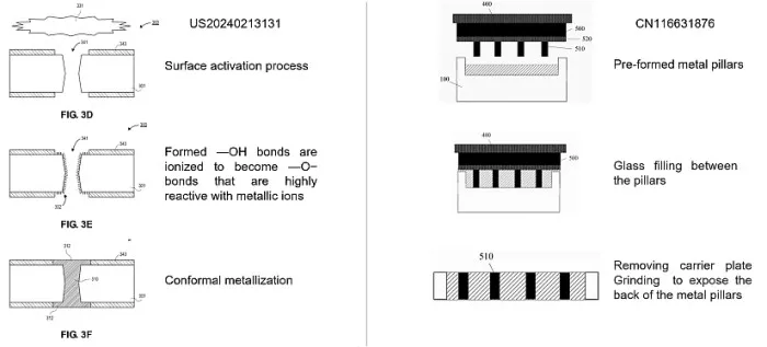
More effective heat management within glass core substrate and interposers is an innovation trigger. Intel has disclosed several inventions on this topic. A heat exit path carved inside the glass core substrate, with fluidic channels can enable cooling through the package substrate and not only through the top die, thus avoiding high temperature damaging the electronic devices integrated with glass (see patent US20220406686). Acting at the metallic connection level is also a valuable option, with thermally conductive sleeves deposited around the through-glass vias for improved heat dissipation (US20230088392). Regarding the mechanical stress management and warpage issues, an invention from Huawei discloses the combination of glass substrate and a glass interposer, thus leading to an enhanced coefficient of thermal expansion (CTE) match (CN118431173). Besides, glass surface typology requires improved materials processes. High surface roughness and the high aspect ratios of through-glass vias (TGVs) present significant challenges for conformal metallization. These challenges can be mitigated through direct plating methods, which eliminate the need for a seed layer, therefore avoiding the formation of voids in the metallic via (Figure 3, US20240213131). Interestingly, other inventions propose the use of prefabricated copper pillars assembled with glass through a reflow process, encapsulating the pillars within glass. This approach, patented by SJ Semi (Figure 3, CN116631876) and Sky Semiconductor (CN118412319), eliminates the need for complex and costly electroplating. Moreover, this glass interposer (adaptor plate) fabrication process offers additional advantages, such as precise control over the via diameter of through-holes and reduced roughness of the glass hole sidewalls, enhancing adhesion and overall manufacturing efficiency. All these innovations highlight efforts to address technical challenges while streamlining production processes, accounting for the recent rise in patent filings.

Figure 3: Examples of patent publications related to the formation of metallic vias inside the glass material.
Advancements in glass integration for photonics
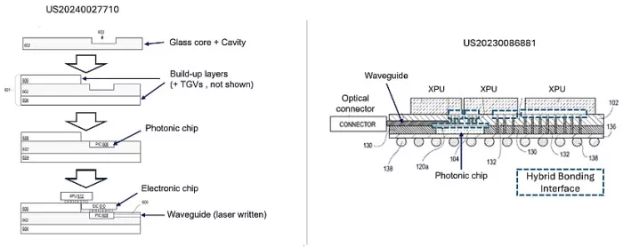
Glass’s outstanding transparency across a wide range of wavelengths makes it an excellent choice for optical signal transmission and Intel is the most prolific patent applicant on this theme. The patent application US20240027710 (Figure 4) features a photonic integrated circuit (PIC) embedded within the glass core of a substrate, seamlessly integrated with an electronic integrated circuit (EIC). This design also incorporates a waveguide within the glass, enhancing optical coupling and enabling thinner, more efficient packaging solutions. Hybrid bonding, a cutting-edge bonding technique utilized in the advanced semiconductor packaging industry (see KnowMade’s Hybrid Bonding Patent Landscape report) is now effectively implemented in glass core substrates. The patent US20230086881 from Intel illustrates a double-sided glass substrate with a PIC that leverages hybrid bonding (Figure 4). The PIC connects to multiple XPUs via TGVs in the glass core substrate, eliminating the need for solder balls. By replacing solder connections with direct metal-to-metal bonding, the photonic device benefits from finer TGV pitch, improved signal transmission, and enhanced heat management at the connection interface.

Figure 4: Examples of patent publications involving the integration of glass core substrate for photonics applications.
Tracking patents on advanced packaging
By analyzing patents, the technological evolution and competitive landscape in advanced semiconductor packaging can be effectively monitored. Recent patent trends reveal significant R&D activities and surge in innovation for glass-based packaging solutions, targeting applications such as Artificial Intelligence (AI), High-Performance Computing (HPC), and photonic integration. As the competitive landscape evolves, companies like Intel and Absolics are leading the way, while numerous players, including Samsung, SJSemi, Xiamen Sky Semiconductor, and Huawei, are actively entering the field.
At KnowMade, we specialize in transforming patent data into actionable intelligence to support decision-making in R&D, innovation, intellectual property, and investment. We have been monitoring patenting activity and analyzing the IP landscape related to advanced semiconductor packaging for several years. Our analysis reports and monitoring services provide clients with a unique and valuable understanding of the latest innovations and ecosystem evolution. In our Advanced Semiconductor Packaging Patent Monitor, we pay special attention to patents related to glass core substrates, glass interposers, as well as optical interconnects and co-packaged optics.
About the author
Pauline Calka, PhD. works for KnowMade as a patent analyst in the fields of semiconductor manufacturing and advanced packaging. She holds a PhD in Memory from the University of Grenoble Alpes (France), in partnership with the CEA-Leti (France). After an Alexander von Humboldt Postdoc fellowship position at the Technical University of Berlin (Germany) and the Leibniz Institute for High Performance Microelectronics on ReRAM development, Pauline worked five years at ASM International (Belgium) as Senior Process Engineer on thin film development for logic, memory and MEMS, and two years at CEA-Leti as Integration Engineer on imaging CMOS sensors.
About KnowMade
KnowMade is a technology intelligence and IP strategy consulting company specialized in analyzing patents and scientific publications. The company helps innovative companies, investors, and R&D organizations to understand competitive landscape, follow technological evolutions, reduce uncertainties, and identify opportunities and risks in terms of technology and intellectual property.
KnowMade’s analysts combine their strong technology expertise and in-depth knowledge of patents with powerful analytics tools and methodologies to turn patent information and scientific literature into actionable insights, providing high added value reports for decision makers working in R&D, innovation strategy, intellectual property, and marketing. Our experts provide prior art search, patent landscape analysis, freedom-to-operate analysis, IP due diligence, and monitoring services.
KnowMade has a solid expertise in Compound Semiconductors, Power Electronics, Batteries, RF Technologies & Wireless Communications, Solid-State Lighting & Display, Photonics, Memories, MEMS & Sensors, Semiconductor Packaging, Medical Devices, Medical Imaging, Microfluidics, Biotechnology, Pharmaceutics, and Agri-Food.
Related Chiplet
- DPIQ Tx PICs
- IMDD Tx PICs
- Near-Packaged Optics (NPO) Chiplet Solution
- High Performance Droplet
- Interconnect Chiplet
Related News
- “From Lab to Fab” – Innovative front-end and advanced packaging technologies for the semiconductor value chain
- YES Selected to Deliver Full Portfolio of Advanced Packaging Tools for Glass Panel AI and HPC Applications by a Leading AI Infrastructure Supplier
- Arm and Meta Deepen Strategic Partnership to Power the Next Era of AI, from Megawatts to Milliwatts, for Billions Worldwide
- PGC Integrates 2.5D/3D Advanced Packaging Technology to Break the “Memory Wall” and Accelerate AI/HPC ASIC Innovation
Latest News
- Kenyi Technologies to collaborate with ADTechnology to co-develop a Server Processor targeting Edge AI and Telco use cases
- Tawazun and Lockheed Martin Sign Strategic Agreement to Establish UAE's Chiplet Design and Assembly Facility
- Xanadu and EV Group partner to build industrial-scale photonic quantum hardware
- AI Optical Interconnect Boom Drives U.S. Firms to Expand Southeast Asia Outsourcing, Opening the Door for Cross-Industry Entrants
- GlobalFoundries accelerates adoption of co-packaged optics for advanced AI data centers with SCALE optical module solution