EV Group Unveils Next-Generation EVG®120 Resist Processing System for High-Volume Manufacturing
New ultra-compact platform adds in-situ resist thickness metrology, wafer edge exposure and EVG®150-class performance in a smaller-scale, highly flexible format
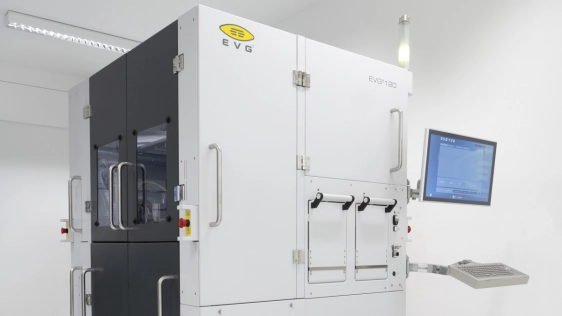
ST. FLORIAN, Austria, February 18, 2026 — EV Group (EVG), a leading provider of innovative process solutions and expertise serving leading-edge and future semiconductor designs and chip integration schemes, today unveiled the next-generation EVG®120 automated resist processing system — a major update to one of the company’s leading coater/developer platforms. Incorporating a new compact architecture, breakthrough capabilities, and design enhancements leveraged from the widely adopted EVG®150 system, the new EVG120 delivers significantly higher throughput, greater flexibility, and improved process control compared to the previous generation. It does all this in a smaller footprint optimized for customers with a high mix of products and resist processes that demand maximum flexibility.
 Ideal for advanced packaging, MEMS, image sensors, photonics, power devices, wafer probe cards, and other fast-growing application areas, the next-generation EVG120 supports spin coating, spray coating and developing of photoresist materials used in photolithography. It accommodates a wide range of substrate types and sizes (from 2 inches up to 200 mm), and supports a variety of resist materials, including thin, thick, positive tone and negative tone, dielectric materials such as PI and PBO, as well as black/color/IR resists for specialty applications.
EVG executives will discuss the next-generation EVG120 platform and other innovative lithography process solutions at the SPIE Advanced Lithography and Patterning (SPIE-AL+P) Conference, taking place next week (February 22-26) in San Jose, Calif.
New Platform, Expanded Capabilities
The EVG120 has been redesigned around a compact 200-mm platform that integrates up to two wet processing modules and 14 bake/chill plates — a 40-percent increase in capacity over the previous-generation platform. The system’s footprint has also been reduced by more than 20 percent, while design improvements enable easier access for tool maintenance and flexible modular configuration.
The system also introduces multiple new capabilities not available on earlier generations, including:
- Wafer Edge Exposure (WEE) – enables selective edge exposure for improved edge accuracy and uniformity
- In-situ Resist Thickness Measurement – enables real-time process monitoring for improved yield and process control (measurement range: 50 nm to 50 micron)
- Enhanced High-Viscosity Dispense System – high-pressure dispensing with closed-loop feedback provides precision coating performance on thick photoresists
- Support for SMIF Loadports – enables cleaner and more efficient material handling
- Stand-by Mode – reduces energy consumption during idle periods; supports SEMI E167 compliance
These additions build upon EVG’s proven coating technologies such as its innovative CoverSpin™ bowl design, which provides superior uniformity and reduces material consumption, and its proprietary OmniSpray® conformal spray coating technology, which provides optimal coating of surfaces with severe topographies and fragile substrates.
“The next-generation EVG120 platform leverages EV Group’s decades of experience in photoresist and lithography processing to support the rapidly diversifying needs of our customers from R&D through volume production,” stated Dr. Thomas Glinsner, corporate technology director at EV Group. “With new capabilities such as in-situ metrology and wafer edge exposure, as well as features inherited from our EVG150 platform, the EVG120 delivers an unmatched combination of coating and developing performance, throughput, flexibility and cost of ownership in a compact, production-ready platform.”
See EVG at SPIE Advanced Lithography
Attendees at SPIE-AL+P interested in learning more about the next-generation EVG120 platform and other innovative lithography process solutions from EVG, are invited to visit EVG at Booth #616 on February 24-25 in the San Jose Convention Center in San Jose, Calif. In addition, EVG is participating in the technical program this year with the following papers:
- “High aspect ratio copper pillar structures enabled by digital lithography patterning of thick resists for AI and HPC device packages” (Wed., Feb. 25, 8:10-8:40am, Room 211B) – presented by Dr. Ksenija Varga, Business Development Manager, EV Group; co-authored with JSR Micro and TECHNIC France
- “Lithography digitalization in semiconductor technologies through advanced software development of high-throughput maskless exposure” (Thu., Feb. 26, 8:00-8:20am, Room 211B) – presented by Alois Malzer, Product Manager, EV Group
- “Ultrasonic spray coating combined with maskless lithography for advanced wafer singulation with complex bump geometries” (Thu., Feb. 26, 9:20-9:40am, Room 210C) – presented by Johanna Rimböck, Scientist, EV Group
- “Exploration and mitigation of local wafer deformations resulting from direct wafer-to-wafer bonding” (Wed., Feb. 25, 5:10-5:30pm, Room 211B) – co-authored with ASML and CEA-Leti
Product Availability
EVG is now accepting orders for the next-generation EVG120 system. Demonstrations are available at EVG’s corporate headquarters. For more information, please visit https://www.evgroup.com/products/lithography/resist-processing-systems/evg120.
About EV Group (EVG)
EV Group (EVG) provides innovative process solutions and expertise for implementing cutting-edge semiconductor designs and 3D integration of microchips. The company’s mission and vision — to be first in new technologies and to support the most advanced applications in micro- and nanotechnology — enable customers to successfully market their new product ideas. EVG’s products, designed for high-volume production, include wafer bonding, lithography, thin-wafer processing, and metrology systems. These solutions drive further advancements in semiconductor frontend scaling, 3D integration, advanced packaging, and other electronics and photonics applications. More information at www.EVGroup.com.
Related Chiplet
- eFPGA Chiplet
- DPIQ Tx PICs
- IMDD Tx PICs
- Near-Packaged Optics (NPO) Chiplet Solution
- High Performance Droplet
Related News
- EV Group Brings Revolutionary Layer Transfer Technology to High-Volume Manufacturing with EVG®850 NanoCleave™ System
- EV Group Advances 300-mm MEMS Manufacturing with Next-Generation GEMINI® Automated Production Wafer Bonding System
- CEZAMAT Boosts Advanced Photonics R&D with State-of-the-Art UV Nanoimprint System from EV Group
- EV Group Hybrid Bonding, Maskless Lithography and Layer Transfer Solutions for Heterogeneous Integration to be Highlighted at ECTC 2024
Latest News
- As AI Moves from Training to Inference, Optics Moves Closer to the Chip
- Arteris Announces Collaboration with IC-Link by imec to Accelerate Next-Gen AI and HPC Silicon
- Asahi Kasei Adds New Slitting Facility for SUNFORT™ to Meet Growing Demand for Advanced Semiconductor Packaging
- ACCM Introduces Celeritas SMC: A Production-Ready, Silicon-Matched Core for Advanced Packaging
- Socionext Addresses Datacenter Infrastructure Customer Demands for Advanced SoCs on TSMC A14 Technology