Advanced Chip Packaging Tools Are New Battleground in India
By Yashasvini Razdan, EETimes | September 16, 2025
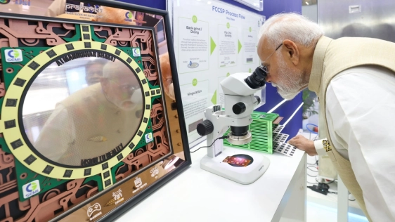
Advanced packaging has become the new battleground in semiconductors. As the industry shifts focus from pursuing smaller transistors to achieving system-level integration, the assembly of bare chips into functional devices becomes crucial.
At SEMICON India 2025, announcements such as the Tata Electronics–Merck MoU for materials and infrastructure, and the Kaynes–Infineon MoU to package Infineon bare die and explore advanced package and MEMS microphone manufacturing in India showed that the country has recognized that packaging is no longer a low-value, outsourced step.
To read the full article, click here
Related Chiplet
- DPIQ Tx PICs
- IMDD Tx PICs
- Near-Packaged Optics (NPO) Chiplet Solution
- High Performance Droplet
- Interconnect Chiplet
Related News
- SK hynix Signs Investment Agreement of Advanced Chip Packaging with Indiana
- Advanced packaging blurs line between monolithic chip and packaged assembly of heterogeneous chips: NAPMP NoI
- Biden-Harris Administration Announces CHIPS Incentives Awards with Absolics and Entegris to Support Development of Advanced Packaging Technology and Onshore Materials for Leading-Edge Chip Production
- ASE Expands its Chip Packaging and Testing Facility to Enable Next-Gen Applications
Latest News
- Avicena Launches the World’s First microLED Optical Interconnect Evaluation Kit for AI Infrastructure Innovators
- Lightmatter Achieves Record 1.6 Tbps Per Fiber to Accelerate AI Optical Interconnect
- Arm Positions Neoverse for AI and Telco Networks at MWC
- NVIDIA Compute Architecture Paves the Way for Scale-Up Optical Interconnects; CPO Penetration in AI Data Centers Expected to Rise Steadily
- CEA-Leti and NcodiN Partner to Industrialize 300 mm Silicon Photonics for Bandwidth-Hungry AI Interconnects