Report: SK Hynix mulls offering advance packaging foundry service
By Peter Clarke, eeNews Europe ( December 16, 2024)
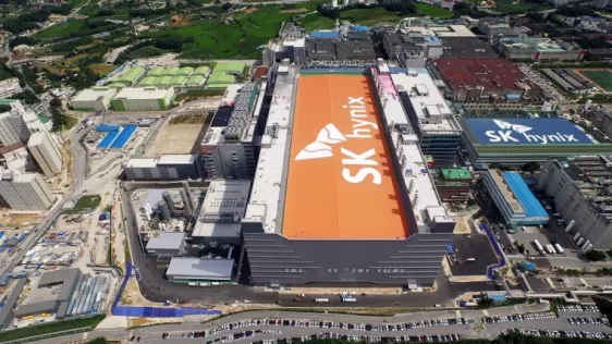
Memory chip vendor SK Hynix is considering a move into 2.5D chip packaging as a foundry outsource operation, according to South Korea’s ETnews.
The move may be partially driven by SK Hynix’s sub-ordinate role to foundry TSMC in the creation of AI accelerators for Nvidia. If SK Hynix could offer 2.5D packaging skills it could potentially offer to work in parallel with TSMC and perform the integration of GPU die and high-bandwidth memory (HBM) DRAM components in AI acceleration components.
To read the full article, click here
Related Chiplet
- Integrated voltage regulator (IVR) chiplet
- High-performance connectivity chiplets
- eFPGA Chiplet
- DPIQ Tx PICs
- IMDD Tx PICs
Related News
- SK hynix Signs Investment Agreement of Advanced Chip Packaging with Indiana
- 2.5D/3D chip technology to advance semiconductor packaging
- 2.5D Integration: Big Chip Or Small PCB?
- SK hynix Partners with TSMC to Strengthen HBM Technological Leadership
Latest News
- Tessolve and Intel Foundry Collaborate on Enablement for EMIB Advanced Packaging Technology
- Intel and Lens Technology Collaborate to Enable Advanced Semiconductor Packaging for the AI Era
- Amkor Technology Announces Strategic Partnership with NVIDIA to Expand Advanced Packaging and Test for Next-Generation AI Infrastructure
- Synopsys Enables AMD Instinct™ MI455X GPU Design with Comprehensive Multi-Die Solution
- AI Data Centers Push Silicon Photonics Toward 300-mm Scale