2.5D/3D chip technology to advance semiconductor packaging
A team of researchers from the Institute of Science Tokyo (Science Tokyo), Japan, has conceptualised an innovative 2.5D/3D chip integration approach called BBCube.
By Jean-Pierre Joosting, eeNews Europe | June 23, 2025
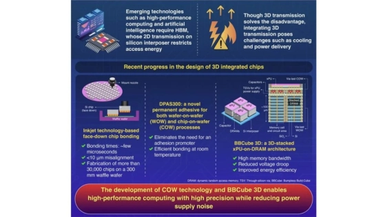
Traditional system-in-package (SiP) approaches, where semiconductor chips are arranged in a two-dimensional plane (2D) using solder bumps, have size-related limitations, warranting the development of novel chip integration technologies. For high-performance computing, the researchers developed a novel power supply technology by employing a 3D stacked computing architecture, which consists of processing units placed directly above stacks of dynamic random-access memory, marking a significant advance in 3D chip packaging.
To implement BBCube, the researchers developed key technologies involving precise and high-speed bonding techniques and adhesive technology. These new technologies can help address the demands of high-performance computing applications, which require both high memory bandwidth and low power consumption, with reduced power supply noise.
To read the full article, click here
Related Chiplet
- Integrated voltage regulator (IVR) chiplet
- High-performance connectivity chiplets
- eFPGA Chiplet
- DPIQ Tx PICs
- IMDD Tx PICs
Related News
- Amkor Technology Breaks Ground on New Semiconductor Advanced Packaging and Test Campus in Arizona; Expands Investment to $7 Billion
- PGC Integrates 2.5D/3D Advanced Packaging Technology to Break the “Memory Wall” and Accelerate AI/HPC ASIC Innovation
- Veeco Announces Multiple Orders for Wet Processing and Lithography Systems to Support Advanced Packaging and Silicon Photonics at a Leading Semiconductor Foundry
- “From Lab to Fab” – Innovative front-end and advanced packaging technologies for the semiconductor value chain
Latest News
- AI Data Centers Push Silicon Photonics Toward 300-mm Scale
- TYLsemi De-Risks Chiplets With New Business Model
- Cadence Introduces AuraStack AI Super Agent, the World’s First Agentic AI Platform for PCB and Advanced Packaging
- Saras Micro Devices Strengthens Senior Leadership Team to Scale Advanced Packaging Technology and Customer Growth
- TYLsemi Raises $43 Million to Launch First Full-Stack Chiplet Platform for Custom AI Silicon