Intel and Lens Technology Collaborate to Enable Advanced Semiconductor Packaging for the AI Era
Collaboration combines Intel's advanced packaging expertise with Lens Technology's precision glass processing capabilities to deliver enhanced performance for future AI and datacenter workloads
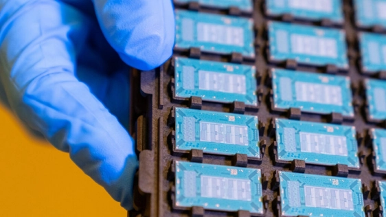
SANTA CLARA, Calif. & CHANGSHA, China — July 24, 2026 — Intel Corporation and Lens Technology today announced a strategic collaboration focused on enabling new technologies for advanced semiconductor packaging. Through this work, the companies intend to explore opportunities to accelerate the development of glass substrate-based packaging solutions that can help enable higher performance, increased interconnect density, and improved power efficiency for future computing platforms. Intel and Lens Technology will leverage their respective strengths in advanced semiconductor packaging, precision manufacturing, glass substrate R&D, and process innovation to support the growing demands of AI, data center, and specialized computing applications.
 “Advanced packaging is becoming a critical driver of semiconductor innovation as AI systems continue to push the boundaries of performance, scale, and efficiency," said Lip-Bu Tan, CEO of Intel. “Intel brings deep expertise in semiconductor architecture and advanced packaging technologies, while Lens Technology contributes world-class capabilities in precision glass processing, laser manufacturing, and large-scale production. Together, we have an opportunity to explore new approaches to advanced packaging that can help unlock the next generation of system-level innovation for the AI era.”
“Lens Technology has built its leadership on advanced materials engineering and precision manufacturing, serving some of the world's most demanding technology companies,” said June Chau, founder and chairwoman of Lens Technology. “By combining Lens Technology's expertise in glass materials, high-precision laser processing, and advanced manufacturing with Intel's leadership in semiconductor design and packaging, we believe we can help accelerate innovation in advanced packaging technologies. This collaboration will support the rapid development of next-generation computing solutions and AI infrastructure for customers around the world.”
Through this collaboration, Intel and Lens Technology will explore potential areas of cooperation in critical manufacturing processes to scale the adoption of advanced semiconductor packaging. Intel and Lens Technology also see meaningful opportunities to collaborate in additional areas where their capabilities may complement one another. Potential areas of future interest include components for AI PCs, high-reliability structural and thermal solutions for data center servers, and hardware platforms supporting AI robotics, intelligent industrial equipment, and edge computing.
Related Chiplet
- Optical Chiplet
- Reverse Gearbox Chiplet
- FlexGen Multi-Die Smart Network-on-Chip (NoC) IP
- Ncore Multi-Die Interconnect IP
- Integrated voltage regulator (IVR) chiplet
Related News
- ASE Launches Automated 310mm Panel-Level Packaging to Accelerate AI Innovation
- Global Semiconductor IDM Qualifies Veeco Wet Processing Platform for Two New Applications in Advanced Packaging
- Siemens and Intel Foundry advance their collaboration to enable cutting-edge integrated circuits and advanced packaging solutions for 2D and 3D IC
- Arteris Joins Intel Foundry Accelerator Ecosystem Alliance Program to Support Advanced Semiconductor Designs
Latest News
- Innolux's Deployment of Key FOPLP Technologies: Leading Next-Gen Advanced Packaging and Seizing AI Opportunities
- Wiwynn, Ayar Labs, and GUC Advance Co-Packaged Optics with Live Demonstration of Integrated Optical Compute System at OCP Global Summit 2026
- ForwardEdge ASIC Announces UCIe 3.0 IP Solution to Accelerate Next-Generation Chiplet-Based ASIC Innovation
- Eliyan Introduces NuLight™: World’s First 2D microVCSEL Interconnect Solution to the Copper Wall
- Evatec delivers first CLUSTERLINE® 310 for Advanced Packaging on small panel formats