Lorentz Solution Jointly Presents with NVIDIA on Automated Large-Scale Chip-Level 3D EM Extraction and Sign-off of Ultra-High-Speed Silicon Photonics and IC/3DIC Designs at 2026 TSMC OIP
PeakView®'s automated xLEM™ flow extends Lorentz's 3D EM leadership from design to full-chip EM sign-off, delivering complete, LVS-clean electromagnetic verification for today's and next-generation ultra-high-speed AI, photonics and IC/3DIC designs
SANTA CLARA, Calif.-- September 14, 2026 -- Lorentz Solution, Inc., the world's leading provider of 3D electromagnetic (EM) design platforms for IC, 3DIC, and advanced packaging, today announced that it is jointly presenting with NVIDIA at the TSMC 2026 Open Innovation Platform (OIP) Ecosystem Forum, to be held on Sept 23, 2026 in Santa Clara, CA. Their paper, "Large-scale Chip-level 3D EM Extraction and Sign-off of Ultra-high-speed Silicon Photonics and Custom Silicon IC/3DIC Designs with PeakView®," marks the third consecutive year that Lorentz™ and NVIDIA will present cutting-edge EM technologies for real silicon designs at TSMC OIP.
 AI data centers are evolving into large-scale distributed compute fabrics, where millions of accelerators operate as a single system connected by ultra-high-bandwidth optical and co-packaged interconnects. At multi-terabit data rates, interconnects behave as distributed electromagnetic structures, and conventional RC-based parasitic verification fails to capture critical inductive effects, EM isolation, and lossy signal propagation. Chip-level EM sign-off verifying the true electromagnetic impact of every critical interconnect has become essential to first-silicon success.
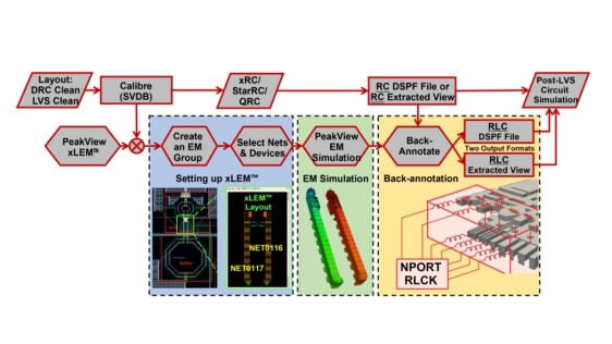
PeakView®'s xLEM™ technology answers this challenge by extending traditional parasitic extraction into a fully automated, chip-level 3D fullwave EM extraction and back-annotation flow in the latest advanced IC and 3DIC nodes. Working directly from the LVS database, xLEM™ preserves connectivity across any design hierarchy, requires no schematic or layout rework, and automatically back-annotates up to thousands of ports with S-parameter and parasitic inductance models up to terahertz with no missing pieces and no double counting. The real custom-silicon sign-off cases presented in the paper demonstrate that automated, full-physics EM sign-off is now practical at chip level for the most advanced ultra-high-speed and silicon photonics designs.
"For the third consecutive year, Lorentz is presenting with NVIDIA at the TSMC OIP Forum, advancing breakthrough EM design and signoff technologies for ultra-high-speed, energy-efficient data movement and computation for AI systems," said Jinsong Zhao, President and Founder of Lorentz Solution, Inc. "For decades, Lorentz™ has pioneered advanced electromagnetic EDA software, supporting generations of semiconductor innovations. Today marks another milestone in our journey to advance innovation and deliver the advanced design capabilities required for the AI era. With xLEM™, PeakView® stands as the industry's ultimate 3D EM design and sign-off platform."
About Lorentz Solution, Inc.
Based in Silicon Valley, Lorentz Solution, Inc. is the world's leading supplier of 3D electromagnetic (EM) simulation and design solutions for IC, 3DIC, and advanced packaging. Learn more at www.lorentzsolution.com.
Related Chiplet
- FlexGen Multi-Die Smart Network-on-Chip (NoC) IP
- Ncore Multi-Die Interconnect IP
- Integrated voltage regulator (IVR) chiplet
- High-performance connectivity chiplets
- eFPGA Chiplet
Related News
- Lorentz Solution Jointly Presents with NVIDIA on Large-Scale 3D Terahertz EM Simulation for Real IC/3DIC Silicon Case Studies in Photonic Switches at 2025 TSMC OIP
- TSMC and Cadence Collaborate to Deliver AI-Driven Advanced-Node Design Flows, Silicon-Proven IP and 3D-IC Solutions
- Chiplet Pioneer Eliyan Achieves First Silicon in Record Time with Implementation in TSMC 5nm Process, Confirms Most Efficient Chiplet Interconnect Solution in the Multi-Die Era
- Marvell Demonstrates Industry’s First 200G 3D Silicon Photonics Engine to Scale Accelerated Infrastructure
Latest News
- Chiplets at the Edge: How Modular SoCs Redefine Performance Per Watt
- Visitech Launches 1-micron Maskless Photohead for Advanced Packaging
- GlobalFoundries reaches agreement to establish U.S.-based supply of silicon interposers for advanced AI packaging
- Applied Materials and Intel Collaborate to Accelerate Chipmaking Innovations for AI-Driven Computing
- BOS Semiconductors to Support MIRISE Technologies’ Automotive Chiplet R&D Project