Diamond Quanta Announces Adamantine Thermal™, Extending Its Advanced Packaging Roadmap Following CES 2026
MOUNTAIN VIEW, Calif.-- January 19, 2026 -- Diamond Quanta today announced Adamantine Thermal™, an engineered-diamond thermal platform designed for integration into advanced packaging workflows and heterogeneous semiconductor systems. The announcement builds on the company’s CES 2026 Eureka Park debut and reflects growing customer interest in diamond-enabled solutions for next-generation electronics.
 The announcement follows Diamond Quanta’s CES 2026 debut, where the company demonstrated 300 mm diamond-on-silicon wafer technology, designed for wafer-to-wafer (W2W) and chip-to-wafer (C2W) bonding compatibility, along with its first commercial diamond glass product, Adamantine Optics™. At CES, the company engaged with system OEMs, semiconductor manufacturers, and ecosystem partners around practical insertion points for diamond within advanced packaging flows.
Extending Diamond Quanta’s CES 2026 Demonstrations
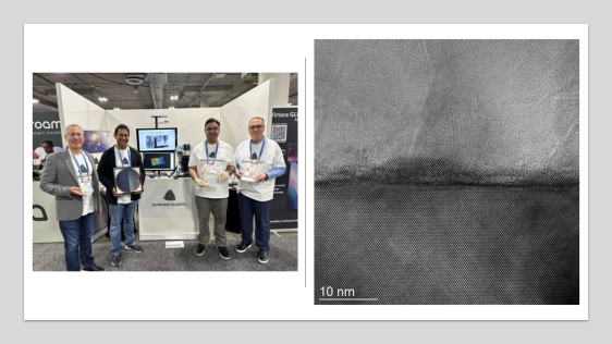
Adamantine Thermal builds directly on the same engineered-diamond manufacturing approach introduced at CES. While diamond is well known for its high intrinsic thermal conductivity, its integration into modern semiconductor packaging has historically been limited by surface roughness, bonding compatibility, and manufacturability at scale.
Diamond Quanta’s approach addresses these challenges by combining:
- CMOS-compatible, low-temperature diamond growth on industry-standard substrates
- Laser-based densification to produce smooth, bond-ready diamond surfaces
- W2W and C2W bonding workflows that support integration into advanced packaging stacks
“Thermal is the most immediate and universal entry point for diamond in electronics,” said Adam Khan, Founder and CEO of Diamond Quanta. “Once diamond can be bonded reliably and at scale, it stops being a research material and becomes a practical platform.”
A key application area for Adamantine Thermal is engineered-diamond glass interposers, where diamond is integrated with glass cores that are already entering advanced packaging workflows. Glass interposers are gaining traction for signal integrity and dimensional stability, and the addition of diamond enables more uniform thermal management while improving flatness and mechanical robustness.
Adamantine Thermal is architected from the outset to support W2W and C2W bonding approaches that are critical for next-generation interposers and stacked systems. By maintaining compatibility with standard fab infrastructure and panel-scale workflows, the platform is designed to bridge today’s passive thermal materials and future diamond-enabled electronic architectures.
Diamond Quanta confirmed that Adamantine Thermal is entering partner evaluation programs, with engineered-diamond interposer concepts advancing in alignment with industry adoption cycles for advanced packaging. The thermal platform complements the company’s recently launched Adamantine Optics offering and reinforces a broader roadmap spanning thermal management, photonics, interposers, and future diamond-enabled systems.
ABOUT DIAMOND QUANTA
Based in Mountain View, California, Diamond Quanta is a materials and semiconductor enablement company developing an engineered-diamond platform designed to integrate into existing semiconductor manufacturing workflows. The company focuses on addressing system-level constraints in advanced electronics, including thermal management and optical performance, through scalable, manufacturable diamond-based solutions. Diamond Quanta’s mission is to make diamond as accessible to the world as silicon. The Physics of Forever™. Learn more at www.diamondquanta.com or contact info@diamondquanta.com.
Related Chiplet
- Integrated voltage regulator (IVR) chiplet
- High-performance connectivity chiplets
- eFPGA Chiplet
- DPIQ Tx PICs
- IMDD Tx PICs
Related News
- Advanced IC Packaging: The Roadmap to 3D IC Semiconductor Scaling
- Qnity Strengthens Long-Term Innovation and Advanced Packaging Roadmap
- Silicon Box welcomes European Commission approval of €1.3 billion Italian State aid measure to support new advanced packaging facility in Novara
- SJSemi closed $700M new financing to further boost its Advanced Packaging projects
Latest News
- GlobalFoundries signs letter of intent with the U.S. Department of Commerce for a $300 million award to accelerate U.S. silicon photonics leadership
- Qnity Strengthens Long-Term Innovation and Advanced Packaging Roadmap
- Multibeam Secures First Taiwan Order for Newly Launched MBX Platform – The Company’s Second Generation Multi-Column E-Beam Lithography System
- From Co-Packaged Optics to Nanolasers: Photonics Moves Inward
- NVIDIA and Broadcom Begin Volume Ramp of CPO Switches, with Optical Engine Yield and Advanced Packaging Capacity Emerging as Key Expansion Bottlenecks