Co-packaged Optics and Optical Interconnects: A Global Picture of the IP Competition
SOPHIA ANTIPOLIS, France – January 21, 2026 – KnowMade, a leading provider of patent analysis services, is proud to announce the release of its latest report, Co-Packaged Optics and Optical Interconnects Patent Landscape Analysis. This comprehensive report provides a detailed examination of the competitive landscape of the co-packaged optics (CPO) and optical interconnects (I/O) technology from a patent perspective, offering critical insights for stakeholders and decision-makers.
A Technological Trend To Watch
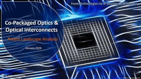 Co-packaged optics (CPO) and optical interconnects (I/O) technologies are emerging as key enablers for next-generation high-performance computing (HPC) and data center architectures. As electrical interconnects approach their fundamental limits, integrating optical interfaces closer to switching and compute silicon offers significant gains in bandwidth density, power efficiency, and scalability. This report analyzes the intellectual property (IP) landscape surrounding CPO and optical I/O solutions, highlighting key patent holders, technological trends, competitive dynamics, and innovation pathways shaping the future of advanced semiconductor packaging.
Key Highlights Of The Report
- Patent Analysis: The report provides an evaluation of the global patent landscape, encompassing patent filing trends, geographical distribution, and legal status.
- Competitive Intelligence: Identification and profiling of major IP players, including both established patent assignees and emerging patent applicants, revealing their R&D focus and strategic positioning.
- Technological Innovations: Insights into the latest technological advancements and innovative approaches, highlighting ongoing R&D efforts and potential future directions.
- Strategic Guidance: Actionable IP intelligence for industrials, enabling informed strategic decisions related to R&D investments, patent portfolio management, and competitive positioning.
The Co-Packaged Optics and Optical Interconnects Patent Landscape report is an essential resource for semiconductor companies, IP professionals, investors, and technology developers aiming to gain a competitive edge in the advanced packaging domain.
Related Chiplet
- Optical Chiplet
- Reverse Gearbox Chiplet
- FlexGen Multi-Die Smart Network-on-Chip (NoC) IP
- Ncore Multi-Die Interconnect IP
- Integrated voltage regulator (IVR) chiplet
Related News
- Wiwynn, Ayar Labs, and GUC Advance Co-Packaged Optics with Live Demonstration of Integrated Optical Compute System at OCP Global Summit 2026
- How can in-package optical interconnects enhance chiplet generative AI performance?
- How does UCIe on chiplets enable optical interconnects in data centers?
- NTT looks to 15Tbit/s chiplet optical interconnects
Latest News
- Innolux's Deployment of Key FOPLP Technologies: Leading Next-Gen Advanced Packaging and Seizing AI Opportunities
- Wiwynn, Ayar Labs, and GUC Advance Co-Packaged Optics with Live Demonstration of Integrated Optical Compute System at OCP Global Summit 2026
- ForwardEdge ASIC Announces UCIe 3.0 IP Solution to Accelerate Next-Generation Chiplet-Based ASIC Innovation
- Eliyan Introduces NuLight™: World’s First 2D microVCSEL Interconnect Solution to the Copper Wall
- Evatec delivers first CLUSTERLINE® 310 for Advanced Packaging on small panel formats