CEZAMAT Boosts Advanced Photonics R&D with State-of-the-Art UV Nanoimprint System from EV Group
New EVG®6200 NT platform enables high-resolution, scalable fabrication of next-generation micro- and nanostructures
WARSAW, Poland and ST. FLORIAN, Austria – April 21, 2026 – CEZAMAT, a world-class research center for advanced materials and technologies, and EV Group (EVG), a leading provider of innovative process solutions and expertise serving leading-edge and future semiconductor designs and chip integration schemes, today announced that CEZAMAT’s research infrastructure has been enhanced with the installation of a new EVG®6200 NT SmartNIL® UVnanoimprint lithography (UV-NIL) system.
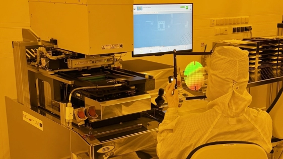 The EVG6200 NT system provides state-of-the-art mask alignment technology combined with industry-leading UV-NIL capability. EVG’s proprietary SmartNIL technology incorporates multi-use soft-stamp processing, enabling unmatched throughput and scalability while supporting the patterning of high-resolution, high-topography structures.
At CEZAMAT laboratories, the EVG6200 NT will be used for the replication and scaling of a wide range of developed micro- and nanostructures. These include diffractive optical elements and various micro-optical components – such as lenses, waveguides and gratings – for use in photonic integrated circuits, detectors and free-space optics.
“We believe that this investment from the Competence Centre for Microelectronics and Photonics project, funded by the National Recovery and Resilience Plan (KPO), will enhance our capabilities, strengthen our collaborations and further establish CEZAMAT as a leading nanotechnology R&D facility. Our expectations and enthusiasm are high as we embark on this significant enhancement of our equipment capabilities,” stated Piotr Wiśniewski, research assistant professor and head of the Intelligent Semiconductor Systems Department (SEMINSYS) at CEZAMAT.
According to Dr. Thomas Glinsner, Corporate Technology Director of EV Group, “We are proud to support CEZAMAT as they expand their capabilities and build on more than a decade of successful collaboration. Europe continues to be a key hub for semiconductor and photonics innovation, and institutions like CEZAMAT play a vital role in advancing next‑generation device manufacturing across the region.”
About CEZAMAT
Centre for Advanced Materials and Technologies CEZAMAT is a multidisciplinary research and development center in Europe, established to effectively bridge advanced scientific research with industrial implementation and commercialization. As the flagship research center of the Warsaw University of Technology, CEZAMAT operates at the intersection of industry, academia, and government, serving as a catalyst for transformative change that benefits society and strengthens the country’s technological sovereignty in strategic dual-use domains. Our expertise encompasses semiconductors, photonics, microelectronics technologies, as well as biotechnology and bioengineering. Located in the heart of Europe, CEZAMAT operates from state-of-the-art facilities in Warsaw that enable advanced research, prototyping, technology validation and small- to medium-batch manufacturing. More information at https://cezamat.pw.edu.pl/home/
About EV Group (EVG)
EV Group (EVG) provides innovative process solutions and expertise that serve leading-edge and future semiconductor designs and chip integration schemes. The company’s vision of being the first in exploring new techniques and supporting next-generation applications of micro- and nanofabrication technologies enables customers to successfully commercialize new product ideas. EVG’s high-volume-manufacturing-ready products, which include wafer bonding, lithography, thin-wafer processing and metrology equipment, enable advances in semiconductor front-end scaling, 3D integration and advanced packaging, as well as in other electronics and photonics applications. More information at www.EVGroup.com
Related Chiplet
- eFPGA Chiplet
- DPIQ Tx PICs
- IMDD Tx PICs
- Near-Packaged Optics (NPO) Chiplet Solution
- High Performance Droplet
Related News
- EV Group Brings Revolutionary Layer Transfer Technology to High-Volume Manufacturing with EVG®850 NanoCleave™ System
- EV Group Advances 300-mm MEMS Manufacturing with Next-Generation GEMINI® Automated Production Wafer Bonding System
- EV Group Unveils Next-Generation EVG®120 Resist Processing System for High-Volume Manufacturing
- EV Group Hybrid Bonding, Maskless Lithography and Layer Transfer Solutions for Heterogeneous Integration to be Highlighted at ECTC 2024
Latest News
- As AI Moves from Training to Inference, Optics Moves Closer to the Chip
- Arteris Announces Collaboration with IC-Link by imec to Accelerate Next-Gen AI and HPC Silicon
- Asahi Kasei Adds New Slitting Facility for SUNFORT™ to Meet Growing Demand for Advanced Semiconductor Packaging
- ACCM Introduces Celeritas SMC: A Production-Ready, Silicon-Matched Core for Advanced Packaging
- Socionext Addresses Datacenter Infrastructure Customer Demands for Advanced SoCs on TSMC A14 Technology