AI Chips Shifting from Round to Rectangular
By Alan Patterson, EETimes | October 16,2025
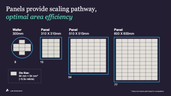
The advanced-packaging needs of AI chips are driving a move by the semiconductor tool and material industry to supply rectangular panels aimed at taking market share from the round silicon wafers we are all so familiar with.
Toolmakers Lam Research and Nikon are among companies selling components for panel production, with an expected business takeoff starting as early as 2027, according to Lam.
Top foundry TSMC, which has dominated advanced packaging of AI chips for customers like Nvidia and AMD, is likely to yield its hegemony of heterogeneous integration to OSATs (outsourced semiconductor assembly and test companies) that are preparing to grab more of the business, according to Lam.
To read the full article, click here
Related Chiplet
- eFPGA Chiplet
- DPIQ Tx PICs
- IMDD Tx PICs
- Near-Packaged Optics (NPO) Chiplet Solution
- High Performance Droplet
Related News
- AI Boom Drives Demand for Ultra-Large Packaging as ASICs Expected to Shift from CoWoS to EMIB, Says TrendForce
- Eliyan Secures $50 Million in Strategic Investments from Leading Hyperscalers and AI Infrastructure Providers to Accelerate Scalable AI Systems
- Siluxtek and GlobalFoundries Forge a Deep Strategic Partnership to Mass-Produce 200G/Lane Silicon Photonic Receiver Chips, Paving the Way for the Industrial Revolution of AI Computing Interconnects
- EdgeCortix Announces New Investment from Axiro Semiconductor and MPower Partners to Advance Next-Generation Edge AI Platforms
Latest News
- As AI Moves from Training to Inference, Optics Moves Closer to the Chip
- Arteris Announces Collaboration with IC-Link by imec to Accelerate Next-Gen AI and HPC Silicon
- Asahi Kasei Adds New Slitting Facility for SUNFORT™ to Meet Growing Demand for Advanced Semiconductor Packaging
- ACCM Introduces Celeritas SMC: A Production-Ready, Silicon-Matched Core for Advanced Packaging
- Socionext Addresses Datacenter Infrastructure Customer Demands for Advanced SoCs on TSMC A14 Technology