Advanced Chip Packaging Tools Are New Battleground in India
By Yashasvini Razdan, EETimes | September 16, 2025
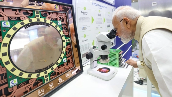
Advanced packaging has become the new battleground in semiconductors. As the industry shifts focus from pursuing smaller transistors to achieving system-level integration, the assembly of bare chips into functional devices becomes crucial.
At SEMICON India 2025, announcements such as the Tata Electronics–Merck MoU for materials and infrastructure, and the Kaynes–Infineon MoU to package Infineon bare die and explore advanced package and MEMS microphone manufacturing in India showed that the country has recognized that packaging is no longer a low-value, outsourced step.
To read the full article, click here
Related Chiplet
- DPIQ Tx PICs
- IMDD Tx PICs
- Near-Packaged Optics (NPO) Chiplet Solution
- High Performance Droplet
- Interconnect Chiplet
Related News
- Biden-Harris Administration Announces CHIPS Incentives Awards with Absolics and Entegris to Support Development of Advanced Packaging Technology and Onshore Materials for Leading-Edge Chip Production
- ASE Expands its Chip Packaging and Testing Facility to Enable Next-Gen Applications
- YES Selected to Deliver Full Portfolio of Advanced Packaging Tools for Glass Panel AI and HPC Applications by a Leading AI Infrastructure Supplier
- Chip Assembler ASE Sees Advanced Packaging Sales Doubling
Latest News
- Quantum Computing Inc. Completes Acquisition of NHanced Semiconductors, Inc.
- GlobalFoundries qualifies SLATE™ advanced packaging technology on 9SW platform for next-generation radio frequency applications
- Qnity Powers the Transition from Shrink to Stack with Advanced Packaging Solutions
- NHanced Semiconductors President Robert Patti to Deliver Plenary Presentation on the Critical Role of Advanced Packaging at the 2026 Lithography Workshop
- Intel Announces Leadership Appointment at Intel Foundry to Accelerate Development and Manufacturing