Scalable Testing of Xanadu’s Canadian made Quantum Photonic Chips with MPI Corporation’s Advanced Electro-Optic Probe Systems

Xanadu’s photonic quantum computing architecture provides several intrinsic advantages over traditional approaches: it operates at room temperature, greatly reducing cooling demands; it supports high qubit connectivity for improved fault-tolerant performance; and it offers a modular, network-compatible structure crucial for scalable quantum systems. Essential components to support future utility-scale, error-corrected quantum computing applications, applicable in bio-medical, optical communications, AI, aerospace and defense industries.
Xanadu currently contributes to the quantum computing ecosystem with systems that use light-based qubits that can be generated, manipulated and entangled on integrated photonic chips. It aims to bring fault tolerant quantum computers to the market by 2029, that can help industries solve real-world problems at unprecedented scale.
These silicon-based EPICs must be characterized under stringent conditions, as even small variations in alignment -affecting optical coupling efficiency and repeatability- or environmental stability can significantly alter device performance such as insertion loss, stability, responsivity, and overall yield. The device portfolio, spanning optical ring resonators, Mach–Zehnder modulators, photodetectors, wavelength-selective filters, and other passive and active photonic components, requires both isolated device testing and integrated subsystem evaluation across full 6-, 8-, and 12-inch wafers.
From a metrology standpoint, several critical challenges arise. High-throughput data acquisition is essential to minimize overall test time, particularly for a densely populated layout. Multi-channel measurement architectures are preferred to support simultaneous characterization of multiple optical device arrays, while parallel testing capabilities help reduce cycle time for large-scale EPIC designs. At the same time, test repeatability is subject to test instrumentation and probe system used, as well as environmental conditions, in addition to mechanical vibration. The latter is especially relevant for Xanadu, which performs wafer-level testing on the 29th floor of a downtown Toronto office tower.
Environmental thermal variability adds another layer of complexity: small temperature fluctuations can impact device characteristics; changes in coupling ratio, refractive index, insertion loss drift, etc. all of which can directly affect the performance of the device under test. MPI’s SENTIO® software addresses these challenges through advanced automation of the optical fiber probe (FAU) calibration process. SENTIO® enables calibration at ambient conditions as well as during temperature-controlled testing (TCT), where wafers are subject to expansion and contraction as a function of temperature. By maintaining precise alignment and compensating for thermal-induced mechanical shifts, SENTIO® ensures compensated optical coupling and consistent measurement performance throughout the full test temperature range.
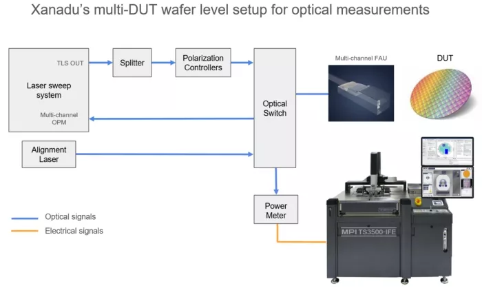
The configuration shown above illustrates the setup used to characterize the optical performance of Xanadu’s grating-based EPICs. A tunable laser serves as the wavelength-dependent source, after which the light is split into multi parallel channels. Each channel passes through a polarization controller to optimize the single-mode state of polarization before it is routed through an optical matrix switch and launched into the grating coupler via a multi-channel optical fiber probe (FAU). The DUT output, collected by the corresponding FAU, is returned through the optical switch and directed into a multi-channel optical power meter. This portion of the configuration is dedicated to optical device characterization.
The second part of the setup supports logic-driven, automated optical probe (FAU) positioning and DUT alignment. This configuration consists of a stationary, power-controlled and polarization optimized laser source combined with a single-channel optical power meter. The analog electrical output of this optical power meter interfaces with the TS3500’s SENTIO® software to enable fully automated alignment.
One of the primary measurements Xanadu performs in this configuration is the characterization of optical insertion loss as a function of wavelength. This wavelength-dependent analysis is essential for validating device-level design performance, identifying fabrication-induced variations, and ensuring that each photonic device meets the requirements needed for large-scale, quantum-ready photonic systems.
Related Chiplet
- eFPGA Chiplet
- DPIQ Tx PICs
- IMDD Tx PICs
- Near-Packaged Optics (NPO) Chiplet Solution
- High Performance Droplet
Related Blogs
- Ultra-high repeatability and ultra-low insertion loss wafer and die-level visible-range E-PIC device characterization using an MPI Corp. probe system, enabled by process optimization from Quantum Transistors
- Accelerate the Photonic IC Design with Cadence EPDA Environment
- Lego-Style Software For Automotive And Industrial Chiplet Systems?
- Arm Zena CSS – Accelerating Chiplet-Based SoC Design for AI-Defined Vehicles
Latest Blogs
- How Intel Foundry Packaging Technologies Redefine AI and HPC Scalability Limits at ECTC 2026
- From complexity to simplicity: Scaling and future-proofing chiplets with AMBA®︎ CHI C2C property negotiation
- High-Speed Heterogeneous Integration with Multiphysics Analysis for TSMC SoW-X
- Chiplet Realization Beyond the Package: Why the Next AI Bottleneck Moves to the Interposer-to-PCB Boundary
- Advancing UCIe Performance: Enabling 40G for Next-Generation Multi-Die Designs