Bridging the Gap to Chiplet Interoperability

The move to multi-die integration brings both promise and complexity. Scalable interconnects and automation are emerging as key enablers of future designs.
 Chiplets have emerged as a dominant theme in discussions of next-generation system architectures. The current narrative describes a vision where design teams can mix and match dies from different sources, using standard interfaces and simplified flows to build multi-die systems.
The analogy to off-the-shelf IP components is often cited, with chiplets expected to become as accessible and interoperable as passives or even microcontrollers. However, while compelling, this narrative is still a long way from reality.
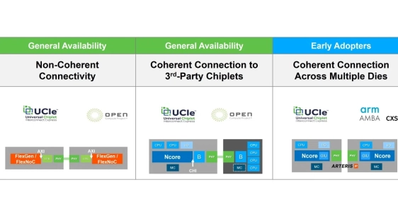
The Current Landscape of Chiplet Integration
Chiplets typically fall into two architectural categories: homogeneous scale-out and heterogeneous disaggregation. Homogeneous designs use multiple identical dies within a package to expand performance capacity, while heterogeneous approaches combine functionally distinct dies tailored to specific roles.
To read the full article on Electronic Design, click here.
Related Chiplet
- eFPGA Chiplet
- DPIQ Tx PICs
- IMDD Tx PICs
- Near-Packaged Optics (NPO) Chiplet Solution
- High Performance Droplet
Related Blogs
- UMI: Extending Chiplet Interconnect Standards To Deal With The Memory Wall
- Embracing the Chiplet Journey: The Shift to Chiplet-Based Architectures
- Chiplet Realization Beyond the Package: Why the Next AI Bottleneck Moves to the Interposer-to-PCB Boundary
- Introduction to Chiplets: Why the Industry is Moving Beyond Monolithic Designs
Latest Blogs
- How Intel Foundry Packaging Technologies Redefine AI and HPC Scalability Limits at ECTC 2026
- From complexity to simplicity: Scaling and future-proofing chiplets with AMBA®︎ CHI C2C property negotiation
- High-Speed Heterogeneous Integration with Multiphysics Analysis for TSMC SoW-X
- Chiplet Realization Beyond the Package: Why the Next AI Bottleneck Moves to the Interposer-to-PCB Boundary
- Advancing UCIe Performance: Enabling 40G for Next-Generation Multi-Die Designs