Chiplet Closure Should Not End at Signoff

A chiplet can meet its individual specifications and the assembled system can still lose the margin required to become a manufacturable product.
The next challenge is carrying design intent through manufacturing, system integration, and product realization.
Chiplet design methodology has advanced rapidly.
Power integrity is evaluated with package behavior. Thermal analysis includes multiple dies and HBM. Mechanical behavior, warpage, interconnect geometry, high-speed channels, and package construction increasingly enter the design flow before hardware exists.
That is progress.
But it also exposes a different problem.
What happens after the models close?
For a heterogeneous package, successful signoff does not automatically establish that the required behavior can be reproduced through fabrication, assembly, test, qualification, and volume manufacturing.
That is where I believe the meaning of closure is beginning to change.
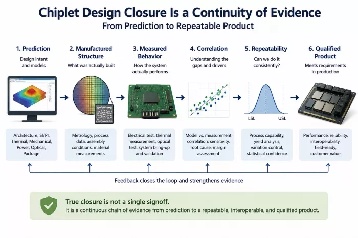
Design closure is becoming the beginning of an evidence chain
Consider a package containing compute chiplets, HBM, high-density die-to-die interfaces, advanced power delivery, and perhaps an optical endpoint.
Before fabrication, engineering teams may already have correlated electrical, thermal, mechanical, and package models.
The design may be internally consistent.
The remaining question is different:
Can manufacturing repeatedly create the physical conditions on which that closure depended?
That question cannot be answered by another nominal simulation alone.
It requires evidence from the hardware that is actually produced.
Metrology establishes what geometry was built.
Electrical test shows what channel was realized.
Thermal characterization shows the actual operating environment.
Assembly data identifies process movement.
Package test reveals interactions not visible at die test.
Qualification shows whether the operating window survives stress and time.
Yield data tells us whether the result is repeatable rather than exceptional.
These are not separate engineering disciplines replacing design analysis.
They are the continuation of closure.
Three realizations follow design closure
I find it useful to separate what happens next into three questions.
1. Manufacturing realization
Can the intended physical structure be produced repeatedly?
For a chiplet package this can involve bond geometry, RDL dimensions, substrate construction, die placement, interconnect formation, material thicknesses, assembly conditions, and other process-dependent parameters.
The important issue is not whether every dimension equals nominal.
It never will.
The issue is whether the manufacturing window produces structures that remain inside the functional window established by design.
That connects two quantities that are often discussed separately:
process capability and product margin.
A dimensional distribution becomes much more meaningful when we know how strongly that dimension influences electrical, thermal, optical, or mechanical performance.
2. System realization
Passing manufacturing inspection still does not prove that the heterogeneous system behaves as intended.
The dies have now become one operating structure.
HBM is active.
Die-to-die links are running.
Power-delivery networks are loaded.
Thermal boundaries have become real rather than prescribed.
If photonics is present, electrical drive, optical coupling, temperature, package mechanics, and test conditions now coexist in one system.
This is where measured behavior needs to be compared with predicted behavior.
Not simply:
Did it pass?
But:
Did the system behave for the reasons we expected?
That distinction matters.
A passing result with unexplained margin movement may be much less valuable than a slightly weaker result whose relationship to design and manufacturing variables is understood.
The second case can be engineered.
The first may merely have worked.
3. Product realization
A successful prototype is still not a product.
The final question is whether the architecture can survive:
unit-to-unit variation
→ lot-to-lot variation
→ operating conditions
→ qualification
→ yield requirements
→ production scale
This is where chiplet economics ultimately become real.
Smaller dies may improve wafer-level yield.
Known-good-die strategies may prevent obviously defective components from entering an expensive assembly.
Advanced bonding may provide extraordinary interconnect density.
None of those advantages alone determines whether the final multi-die product is economically manufacturable.
The relevant quantity eventually becomes something broader:
How much of the designed capability survives repeatedly into qualified products?
This changes how we should think about margin
Traditional signoff produces margins against requirements.
For heterogeneous integration, those margins increasingly need a second interpretation.
Some margin belongs to the design.
Some is consumed by physical realization.
The important question is therefore not merely whether margin exists at signoff.
It is where that margin goes afterward.
For example, suppose a high-speed die-to-die interface closes with adequate electrical margin.
The next useful engineering questions are:
Which manufactured dimensions have the strongest influence on that margin?
What does metrology say those dimensions actually look like across builds?
Does measured electrical behavior move in the direction predicted by the model?
Does the accepted manufacturing window still fit inside the electrical operating window?
Now SI, manufacturing, metrology, and test are no longer four reports.
They become one engineering argument.
That is a much more powerful form of closure.
Photonics makes this especially visible
Optical chiplets provide an excellent example because proximity alone is not the objective.
Moving the electrical-to-optical boundary closer to compute can reduce electrical reach.
But an architecture only becomes valuable if the required electrical geometry, optical coupling, thermal environment, assembly precision, test method, and manufacturing window can be realized together.
A modulator can have excellent device characteristics.
A PIC can demonstrate excellent optical performance.
An electrical interface can close.
Yet the engineering problem is not complete until the integrated optical endpoint can be manufactured, tested, qualified, and reproduced while retaining sufficient system margin.
That is why optical chiplets are not merely adding another die to the package.
They are extending what closure has to prove.
From signoff to continuous closure
This suggests a broader change in methodology.
Today we often think of closure as something achieved before release:
requirements → analysis → optimization → signoff
For increasingly heterogeneous systems, closure may need to become more continuous:
design prediction
→ manufactured structure
→ measured behavior
→ correlation
→ updated understanding
→ production evidence
This is also where intelligence can become much more useful.
AI should not only accelerate architecture exploration or design optimization.
It can help connect information that today lives in different parts of the development flow:
metrology with electrical results,
assembly history with yield,
thermal measurements with package models,
test signatures with physical geometry,
and qualification results with earlier design assumptions.
The objective is not AI-generated signoff.
It is faster evidence-driven convergence between what was designed and what was actually built.
The next chiplet advantage may come from continuity
The industry has already made enormous progress in partitioning systems into chiplets.
The next competitive advantage may come from connecting the stages that follow that partitioning.
Not simply:
Can we design the dies?
or:
Can we assemble the package?
But:
Can we preserve a continuous engineering argument from design intent through manufacturing evidence to qualified product behavior?
That is a different definition of closure.
And as chiplet systems incorporate more HBM, denser die-to-die links, vertical power delivery, 3D integration, and photonics, I believe that definition will become increasingly important.
Design closure establishes what should work.
Manufacturing realization establishes whether we can build it.
System realization establishes whether the integrated hardware behaves as intended.
Product realization establishes whether we can do it repeatedly.
The chiplet era does not make conventional signoff less important.
It makes what comes after signoff impossible to ignore.
© 2026 Moh Kolbehdari. Original technical perspective. All rights reserved.
Related Chiplet
- Optical Chiplet
- Reverse Gearbox Chiplet
- FlexGen Multi-Die Smart Network-on-Chip (NoC) IP
- Ncore Multi-Die Interconnect IP
- Integrated voltage regulator (IVR) chiplet
Related Blogs
- Chiplet, not so fast, did you look at everything?
- What is a Chiplet, and Why Should You Care?
- Cadence Sets the Gold Standard for UCIe Connectivity at Chiplet Summit '24
- Intel® Shows OCI Optical I/O Chiplet Co-packaged with CPU at OFC2024, Targeting Explosive AI Scaling