Accelerating Physical AI Through Cadence Silicon Solutions and Arm Total Design

Physical AI is shifting artificial intelligence from centralized data centers into intelligent systems that must perceive, reason, and act in the real world. Autonomous vehicles, robots, drones, industrial systems, and other autonomous machines all require local intelligence that can process sensor-rich workloads in real time while meeting strict requirements for power, performance, functional safety, cybersecurity, and lifecycle reliability.

Figure 1: Physical AI applications
That shift places new demands on silicon. Physical AI is a systems challenge, requiring a complete foundation that connects AI models to trusted silicon and ultimately to deployable technology. Cadence addresses these current industry challenges through an integrated physical AI solution built around four core pillars: right-sized inference, trusted execution across the lifecycle, standards-based modularity, and one partner from spec to silicon to system.
Arm Total Design for Physical AI reflects the same ecosystem imperative. By bringing together compute platforms, silicon IP, implementation technologies, software, services, and ecosystem partners, Arm Total Design for physical AI creates a collaborative model for building the next generation of AI-enabled systems. For customers, that collaboration matters because physical AI is not solved by a single component. It requires coordinated progress across architecture, software, security, verification, packaging, and silicon realization.
Cadence already plays a pivotal role in the physical AI ecosystem by helping customers move from early architecture exploration to production-ready silicon. Cadence combines AI-driven design, system analysis, verification, digital implementation, multiphysics optimization, IP, advanced packaging, and chiplet realization technologies into a comprehensive development platform. The result is a more complete path for customers that need to accelerate silicon design for physical AI while reducing the integration risk, schedule pressure, and execution complexity of a multi-vendor stack.
A Physical AI Collaboration with Arm Built for Scalable Platforms
Cadence previously announced a comprehensive collaboration with Arm around Arm® Zena™ Compute Subsystems (CSS), helping to address one of the most demanding areas of silicon innovation: scalable, AI-enabled systems that must operate reliably in the physical world. Arm Total Design for Physical AI enhances this collaboration by extending the Cadence solution into a broader ecosystem model that brings together compute platforms, silicon IP, software, virtual platforms, tools, services, sensors, and deployment expertise to reduce integration complexity and accelerate development. As intelligent platforms evolve into software-defined, sensor-rich systems, semiconductor teams must support perception, sensor fusion, planning, control, connectivity, security, and lifecycle management in increasingly complex SoCs and chiplet-based architectures. Cadence’s physical AI silicon solutions, advanced implementation flows, IP, chiplet platform, and system-level expertise, paired with Arm’s ecosystem approach, gives customers a more coordinated path to building, validating, and scaling physical AI systems. This is especially important for systems that require real-time inference, deterministic performance, functional safety, lifecycle trust, and deployment readiness from silicon through system integration.
Right-sized inference for physical AI is critical. Intelligent physical systems do not have a one-size-fits-all compute profile. Some workloads require always-on, low-power inference. Others require higher-performance multimodal processing across cameras, radar, lidar, audio, environmental sensors, and system-state data. By combining Arm’s scalable compute foundation with Cadence technologies for architecture exploration, system analysis, IP integration, and silicon implementation, customers can better tune their designs for the performance, power, area, and latency targets required by their specific applications.
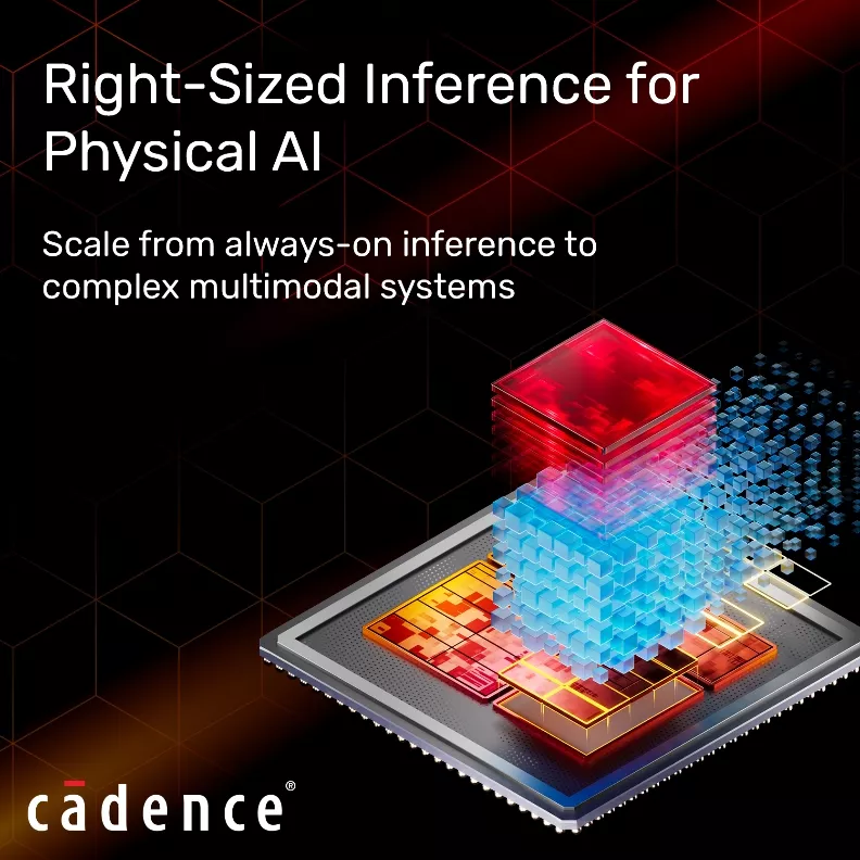
Figure 2: Right-sized inference
These new physical AI systems must have trusted execution across the lifecycle. Physical AI systems operate in mission-critical and safety-sensitive environments and must protect data, software, models, firmware, configuration assets, and device identity from manufacturing through field deployment. In software-defined physical AI systems, this becomes especially important because connected platforms depend on secure boot, authenticated updates, attestation, lifecycle management, and system-level trust. Cadence’s broader physical AI solution, including security capabilities such as Securyzr, provides a foundation for protecting AI workloads, chiplet-based platforms, and connected edge systems throughout their operational life.
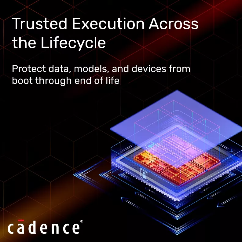
Figure 3: Trusted execution
Physical AI demands are increasing faster than traditional monolithic SoC approaches can comfortably absorb. Chiplet-based architectures offer a scalable path by enabling compute, AI acceleration, memory, I/O, security, and domain-specific functions to be integrated through reusable, interoperable building blocks. Cadence’s physical AI chiplet platform and design expertise, UCIe-based integration capabilities, standards-aligned IP, EDA flows, and multi-die implementation technologies help customers pursue modular architectures that can scale across platforms and product generations while preserving flexibility and reuse. The Cadence physical AI chiplet platform aligns with the OCP Foundational Chiplet System Architecture specification, enabling interoperable chiplets.
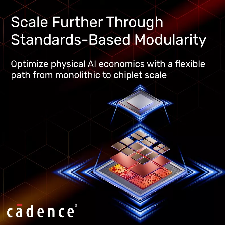
Figure 4: Standards-based modularity
Cadence can help customers translate high-level physical AI requirements into executable silicon specifications, integrate Arm-based compute subsystems with the required IP and system infrastructure, validate software earlier through virtual and hybrid development environments, implement the design, and support the path toward silicon realization. For customers, that means fewer handoff points, less multi-vendor integration risk, and a more direct route from concept to production.
Together, Cadence and Arm are helping customers address the system-level realities of physical AI. The collaboration is not simply about connecting a compute subsystem to an implementation flow, it is about giving silicon innovators a more integrated foundation for building AI-defined systems: scalable compute, trusted execution, standards-based chiplet pathways, early software enablement, and silicon realization expertise in one coordinated ecosystem.
Why This Matters for the Physical AI Era
Physical AI changes the center of gravity for semiconductor design. Customers are no longer optimizing isolated IP blocks or single-purpose SoCs. They are building intelligent systems that must see, reason, and act in real time, often under strict power, safety, cost, and reliability constraints. That requires a systems mindset.
The Cadence physical AI solution addresses the needs of this shift clearly: AI accelerated, secure by design, standards-based, and scalable. This collaboration with Arm reinforces each part. Arm provides a scalable compute foundation for Physical AI systems. Cadence helps customers realize that foundation through software enablement, IP integration, verification, implementation, advanced packaging, chiplet design, and silicon realization services.
Supporting the needs of physical AI applications, Cadence offers a physical AI chiplet platform, which is a configurable, standards-based multi-die solution that accelerates development of scalable physical AI systems by combining pre-verified reference chiplets, UCIe die-to-die connectivity, advanced packaging flows, and a broad Cadence IP portfolio. It integrates system, AI acceleration, and CPU cluster chiplets, anchored by Cadence Neo NPU inference, Arm-based compute, memory, I/O, security, debug, and system-management capabilities, to support demanding workloads across autonomous vehicles, robotics, drones, industrial systems, and other autonomous machines. The platform reduces cost, schedule, and integration risk while enabling package-level scalability, interoperability, and rapid customization for application-specific physical AI silicon.
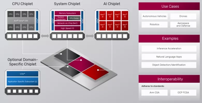
Figure 5: Cadence physical AI chiplet platform
For the market, the value is straightforward. Customers can move faster from model to trusted silicon. They can reduce the risk associated with complex heterogeneous integration. They can explore modular chiplet-based architectures when scale demands it. And they can rely on a coordinated ecosystem rather than stitching together disconnected technologies across the development lifecycle.
As physical AI expands across robotics, drones, industrial systems, intelligent edge platforms, and other real-world AI applications, this model of collaboration will become increasingly important. The next generation of intelligent machines will depend on silicon platforms that combine compute performance, software readiness, lifecycle trust, modular scalability, and production discipline. Cadence is positioned to help customers build those platforms faster, with lower risk, and with a complete path from specification to silicon to system.
Related Chiplet
- Optical Chiplet
- Reverse Gearbox Chiplet
- FlexGen Multi-Die Smart Network-on-Chip (NoC) IP
- Ncore Multi-Die Interconnect IP
- Integrated voltage regulator (IVR) chiplet
Related Blogs
- Cadence Recognized for Accelerating AI and 3D-IC Applications by Samsung Foundry
- Cadence and AVCC to Advance Physical AI Innovations for Autonomous Vehicles
- AMI Outlines Full Support for Arm Total Design Chiplet Architecture to Custom Silicon Designers and Producers at APAC ATD Summit
- From Spec to Silicon: Successful Physical AI System Chiplet Bring-Up
Latest Blogs
- Cooling Is Becoming Part of the Chiplet Architecture
- When AI Moves the World: Building a Chiplet Standard for Physical AI
- Co-Packaged Optics Moves from Promise to Production Planning
- Co-Packaged Optics Moves from Promise to Production Planning
- Co-Packaged Optics Moves from Promise to Production Planning