Building out the Photonic Stack

The fundamental architecture of computers is changing.
In a previous post, I wrote about how we’re approaching the final process node—how Moore’s Law has faltered just as the demand for compute has exploded. The path forward isn’t smaller transistors. It’s assembling maximum-sized chips into datacenter-scale computers, connected by light.
But here’s the thing about building the future: you can’t do it alone. And you can’t do it without solving every layer of the stack.
100X Bandwidth Requires a 100X Light Engine
We’ve spent years demonstrating that our PassageTM photonic interconnect platform can shatter the shoreline bandwidth limitations that constrain today’s interconnects. We’ve proven 16-wavelength bidirectional links on a single fiber. We’ve shown wall-plug efficiency of 4.6 pJ/bit, including SerDes, lasers, photonics and everything else. We’ve validated thermal stability under conditions that would destroy conventional systems.
But even the most advanced photonic interconnect is only as capable as the laser technology that powers it. Just as we’re about to scale optical interconnect bandwidth by 100X, we must do the same with optical power – and conventional discrete lasers cannot get us there.
Today’s co-packaged optics and near-package optics solutions rely on discrete indium phosphide laser diodes integrated into External Laser Small Form Factor Pluggable (ELSFP) modules. These architectures have hit a power wall. Connector end faces and epoxy-bonded assemblies are vulnerable to thermal damage at power levels as low as hundreds of milliwatts. The industry has developed mitigation strategies—expanded beam connectors, hermetic packaging, improved contamination control—but these don’t solve the fundamental scaling problem. You still need more modules, more rack space, more points of failure. Doubling bandwidth means doubling ELSFPs, which doubles cost, power consumption, and front-panel real estate while degrading system-level reliability.
The photonics industry has been working toward CPO for years. What’s been missing is a laser architecture that scales with integration rather than against it.
Announcing Guide™
Today, we’re announcing Guide, the industry’s first VLSP light engine.
The lasers that power CPO and NPO today come in the form of single laser diodes or arrays of up to eight diodes, glued together in a free-space optical chain of lenses, isolators, and other discrete components. It feels a lot like a lab setup—but it’s been surprisingly scalable as the backbone of datacenter laser solutions. The performance gap between single lasers and laser bars is massive, yet the architecture remains fundamentally the same: manual assembly of discrete optics.
At Lightmatter, we’ve been questioning why lasers are built this way. When we think of light, we don’t think of lenses—we think of waveguides. We don’t think about a handful of optical components—we think about tens of thousands.
VLSP—Very Large Scale Photonics—represents our approach applied to lasers. Instead of assembling discrete laser diode modules with lenses, epoxy bonds, and fragile interfaces, VLSP integrates everything into a unified photonic chip, leveraging Lightmatter’s deep expertise in architecting photonic-electronic systems with exquisite control and telemetry. We’re moving laser manufacturing from manual assembly lines toward semiconductor-grade integration.
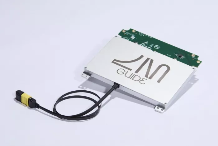
Our Guide validation platform is sampling with customers now. The feedback so far focuses on how impressive the telemetry, power uniformity (0.1 dB across all fibers with 100 mW+ per fiber), absolute wavelength accuracy, and wavelength stabilization (±20 GHz) are for this 16-wavelength laser. This first-of-its-kind module powers a record 51.2 Tbps of bandwidth. When the light engine is this powerful, it makes the design of the photonic links much easier.
An intended side effect of moving from lab-bench style free-space optics integration to processor-like manufacturing and packaging is that Guide is more reliable. VLSP replaces epoxy-bonded components like lenses with integrated photonics. The result is an optical path with no contamination-sensitive optical surfaces exposed to the data center environment. You also need many fewer Guides than discrete laser ELSFP modules. Fewer components are always more reliable.
We’re just getting started with Guide and VLSP. Guide scales from 1 to 64 wavelengths using the same integration approach. Adding wavelengths doesn’t mean adding laser modules. It’s a chip, not a delicate assembly of optical components.
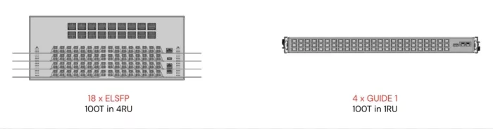
The density improvement is dramatic: the first-generation Guide validation platform enables 100 Tbps of switch bandwidth in a compact 1RU chassis. Achieving equivalent bandwidth with conventional ELSFP modules would require approximately 18 units occupying 4RU— a 4x reduction in rack space with a corresponding reduction in connector count and potential failure points.
Guide + Passage
Guide is designed to work best with Passage. But it’s also available as a standalone product to enable rapid scaling in CPO and NPO bandwidth across the industry.
Our customers are building infrastructure for mixture-of-experts architectures and world models at scales that demand semiconductor-grade integration everywhere, including the light source. We recognize that the transition to CPO will involve many optical engine architectures, not just ours. Guide is designed to be interoperable with third-party NPO and CPO solutions.
The Guide VLSP validation platform is shipping now to multiple partners, with platforms deployed for customer evaluation. Evaluation Kits are available on a priority basis to strategic partners integrating Guide with their optical engine roadmaps.
Building in Taiwan

Great technology needs a great ecosystem to reach its full potential. Taiwan is the center of gravity for advanced semiconductor manufacturing—and increasingly, for advanced packaging, photonic integration, and the full stack required to build CPO at scale.
We’re opening a Lightmatter engineering and business development office in Hsinchu, and hosting Taiwan Tech Day on January 27 – 28, 2026 to engage directly with the ecosystem, analysts and media. We’re hiring in-region teams to support our partnerships and customer engagements across the region.
Assembling the Ecosystem Stack
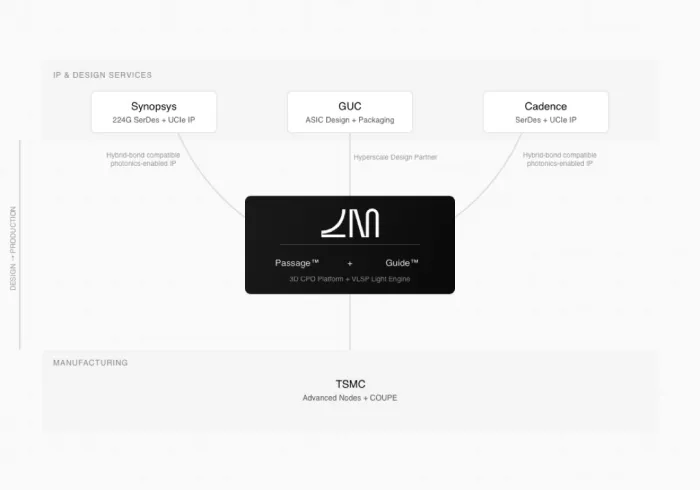
Building production-ready CPO requires solving integration challenges at every layer—from advanced CMOS design to the electrical-to-optical interface to high-volume manufacturing. No single company owns all of these capabilities. Over the past two years, we’ve been building a network of partnerships that spans the full stack—foundries, OSAT providers, IP vendors, EDA companies, and ASIC design houses.
This week, we’re publicly announcing three of these collaborations:
GUC (Global Unichip Corp.) is the advanced ASIC leader and, with TSMC as their largest shareholder, a key enabler for hyperscaler custom silicon. We’re building a chip together. This partnership combines GUC’s ASIC design expertise and advanced packaging capabilities with our photonic interconnect to co-develop commercial Passage CPO solutions for the world’s largest data center operators. This is the concrete path from our demonstrations to hyperscaler silicon.
Synopsys is collaborating with us to adapt their 224G SerDes and UCIe IP for TSMC’s COUPE process—making it hybrid-bond compatible and photonics-enabled for integration into Passage. The goal is an HVM-ready CPO platform that reduces design risk for customers integrating Passage into their XPU and switch designs. We will deliver silicon-proven IP, optimized for the electrical-to-optical interface.
Cadence is working with us to adapt their optics-optimized SerDes and UCIe IP for hybrid bonding and photonic integration. The focus is on fitting CPO into industry-standard packaging workflows—customers shouldn’t have to reinvent their design methodology to adopt photonics. This collaboration establishes a roadmap of silicon-proven connectivity IP that evolves alongside Passage, giving hyperscalers a path to CPO-enabled custom silicon without architectural disruption.
These three represent a pattern of deep technical integration that we’re weaving across the ecosystem. Each collaboration addresses a specific interface that has historically been a barrier to CPO adoption. We’ll have more to announce in the coming quarters.
The Network Is Becoming the Computer
The world has hit a wall in per-silicon-area performance. The network is becoming the computer, and that network needs to run on light.
Guide solves the laser scaling problem. Passage solves the interconnect bandwidth problem. Our ecosystem, including the partners we’re announcing today and many others, solves the integration and manufacturing challenges that stand between today’s demonstrations and tomorrow’s production systems.
The transition to co-packaged optics is no longer a question of if. The supply chain is maturing. The design methodology is coming together. The path to high-volume manufacturing is becoming clear.
The future of AI infrastructure will be built on photonics.
Nick Harris, Ph.D.
Founder and CEO
Related Chiplet
- Integrated voltage regulator (IVR) chiplet
- High-performance connectivity chiplets
- eFPGA Chiplet
- DPIQ Tx PICs
- IMDD Tx PICs
Related Blogs
- Accelerate the Photonic IC Design with Cadence EPDA Environment
- Chiplets: The Building Blocks of Sustainability
- Scoping out the chiplet-based design flow
- Building the Foundation for an Open Chiplet Future: Foundation Chiplet System Architecture (FCSA)
Latest Blogs
- Making chiplets work for AI requires more than connectivity
- When EMC Shielding Must Bend With the Package
- The Bottleneck Isn’t Compute. It’s Getting the Chip Built!
- How Intel Foundry Packaging Technologies Redefine AI and HPC Scalability Limits at ECTC 2026
- From complexity to simplicity: Scaling and future-proofing chiplets with AMBA®︎ CHI C2C property negotiation