3D IC design for the AI era: an EDA perspective

The relentless pursuit of artificial intelligence (AI) innovation has ushered in an era of unprecedented computational demand, pushing the boundaries of traditional silicon architecture. As Moore’s Law decelerates, the industry faces a critical juncture where conventional 2D monolithic designs can no longer meet the escalating requirements for bandwidth, latency, and power efficiency demanded by next-generation AI workloads. In response, 3D IC technology has emerged as a pivotal enabler, offering a pathway to overcome these scaling bottlenecks and unlock new levels of performance. However, this new architectural approach introduces profound design complexities that necessitate a revolutionary approach to EDA, one deeply rooted in industrial-grade AI.
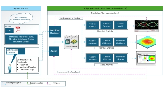 The increasing sophistication of AI, particularly in transformer-based models, underscores a fundamental shift in chip design philosophy. Instead of merely adapting software to existing hardware, the focus has moved to architecting silicon specifically for AI workloads. This “AI-first chip design” paradigm mandates hardware capable of massive parallelism and high-speed data movement, all while adhering to stringent power and thermal limits.
3D IC technology directly addresses these critical demands through the vertical integration of multiple dies, such as High Bandwidth Memory (HBM) with logic, utilizing through-silicon vias (TSVs). This vertical stacking dramatically elevates bandwidth, with HBM4 stacks now delivering up to 3 TB/s per stack, and significantly reduces latency. Such advances are indispensable for the development of advanced AI accelerators and high-performance computing systems.
To read the full article, click here
Related Chiplet
- Optical Chiplet
- Reverse Gearbox Chiplet
- FlexGen Multi-Die Smart Network-on-Chip (NoC) IP
- Ncore Multi-Die Interconnect IP
- Integrated voltage regulator (IVR) chiplet
Related Blogs
- Advancing 3D IC Design for AI Innovation
- Designing the Future We Can Verify: A Vision for Multi-Die Design, STCO, and Trustworthy AI
- Tackling Key HBM and Advanced Packaging Bottlenecks for the AI Era
- Cadence Recognized for Accelerating AI and 3D-IC Applications by Samsung Foundry