3D-IC Packaging: Wafer Stacking, Hybrid Bonding, and Interposer/RDL Techniques

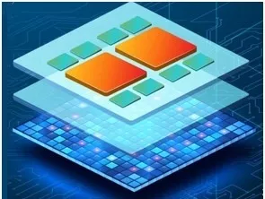
The semiconductor industry is entering a new era where transistor scaling alone can no longer fuel performance gain. With AI accelerators pushing beyond 2–5TB/s of die-to-die bandwidth, hyperscale systems demanding higher compute density, and mobile devices requiring extreme power efficiency, advanced packaging has become the new engine of system innovation.
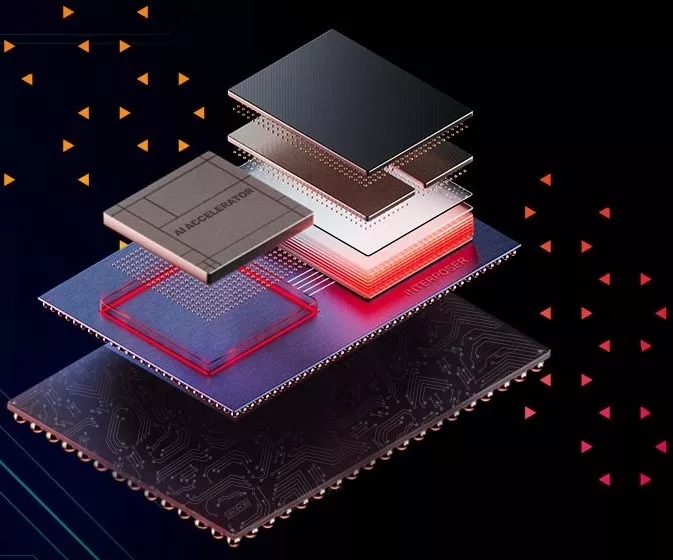
Industry forecasts indicate that the 3D-IC and advanced packaging market will exceed USD 89.9B by 2030, growing at 11.7% CAGR driven by chiplet architectures, silicon interposers, and 3D stacking in memory and logic devices. In other words: packaging is no longer an afterthought—it is the architecture.
This blog breaks down the major 3D-IC packaging methods used today, from wafer stacking flows to hybrid bonding, interposer choices, and package-aware design, and examines how engineers evaluate tradeoffs in density, cost, manufacturability, and reliability.
Wafer-to-Wafer, Die-to-Wafer, and Die-to-Die Flows
3D assembly can follow multiple integration flows, each optimized for different die sizes, yields, and performance requirements.
Wafer-to-Wafer (W2W)
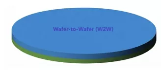 W2W bonding provides the highest throughput but requires matching wafer sizes and similar yields on both wafers. This makes it ideal for:
- Memory-on-memory stacks (e.g., 3D NAND)
- Logic-on-memory configurations with tight alignment
- High-volume applications where wafer-level yields are predictable
Its main limitation is yield-loss multiplication; one bad die can compromise an entire bonded wafer pair.
Die-to-Wafer (D2W)
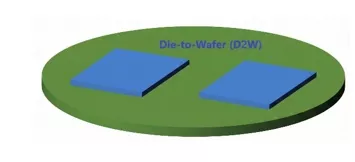 D2W bonding enables the placement of known-good dies on a target wafer, thereby dramatically improving yield for heterogeneous stacks. It's suited for:
- High-value chiplet integrations
- Logic-on-memory with dissimilar die sizes
- Cases where each die has a different reticle or process node
This method improves overall stack yield but is slower than the W2W method.
Die-to-Die (D2D)
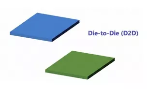 D2D bonding is used when individual chiplets or small dies need extremely tight placement accuracy. Advantages include:
- Highest placement flexibility
- Ideal for high-performance chiplets
- Compatible with both micro-bumps and hybrid bonding
D2D is the most flexible but also the most throughput-limited assembly flow.
Once the proper assembly flow is selected, designers must determine how dies will electrically connect at the interface, setting up the choice between hybrid bonding and micro-bumps.
Hybrid Bonding vs Micro-Bumps: Density and Yield
Interconnect technology defines the achievable bandwidth, power, and thermal behavior of a 3D stack.
Micro-Bumps
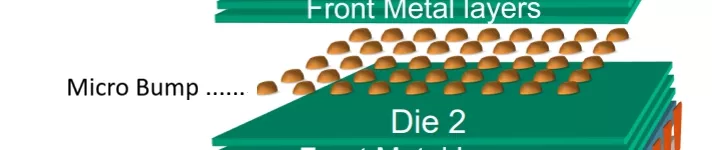
Micro-bumps remain widely used for:
- 2.5D interposer systems
- Early-generation chiplet architectures
- Die stacks that require mechanical compliance
Typical bump pitches range from 35 to 55 µm, with emerging processes nearing 20–25 µm. While reliable and OSAT-friendly, micro-bumps introduce:
- Higher parasitics (R, L, C)
- Larger pitch and lower density
- Solder-joint fatigue risks
Hybrid Bonding
Hybrid bonding enables direct copper-to-copper (Cu-Cu) bonding with no solder, achieving:
- Pitch below 10 µm, approaching <5 µm in development
- Better thermal conduction
- Much lower interconnect impedance
- Higher bandwidth per watt
The enhanced thermal conduction of hybrid bonds can be effectively modeled with tools such as the Celsius Thermal Solver, thereby preventing the formation of hotspots. This capability makes hybrid bonding essential for AI, HPC, and HBM-logic stacking.
Yield Considerations
Hybrid bonding requires extremely tight surface preparation and CMP control, while micro-bumps remain more forgiving. Many OEMs utilize hybrid bonding for performance-critical layers and microbumps elsewhere, thereby creating hybrid integration hierarchies.
As density scales upward, horizontal routing must also evolve. Interposers and RDL structures form the “wiring fabric” bridging dies across the package. Solutions like Cadence Clarity 3D Solver deliver high-accuracy electromagnetic (EM) modeling for complex interconnects across PCBs, IC packages, and System on IC ( SoIC )designs. By identifying EM risks early, Clarity enables more robust multi-die integration and the design of next-generation systems.
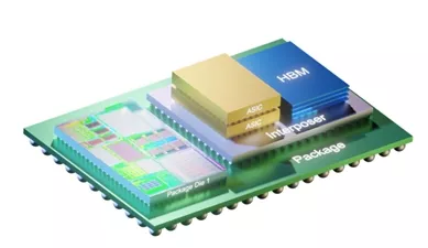
Interposers and RDL: Silicon, Organic, and Glass
Selecting the appropriate interposer or redistribution layer (RDL) structure is crucial for maintaining signal integrity, ensuring power integrity, and minimizing overall cost.
Silicon Interposers (2.5D)
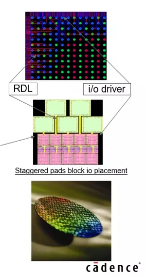 Silicon is the gold standard for:
- Extremely high routing density
- Fine-pitch micro-bump arrays
- High-speed memory interfaces (HBM on logic)
- Superior thermal conductivity
But they are expensive and limited by wafer size constraints.
Organic Interposers
Organic substrates offer:
- Larger panel sizes
- Lower cost
- Sufficient density for many chiplet topologies
However, they have:
- Lower routing density
- Higher warpage and CTE mismatch challenges
Organic RDL is becoming increasingly attractive for mid-range chiplets and AI accelerators that don’t need silicon-level density.
Glass Interposers
Glass is emerging as the “best of both worlds” option:
- Excellent dimensional stability
- Low dielectric loss
- Potential for panel-scale manufacturing
- High-density RDL capability
However, supply chain maturity and tooling availability are still evolving.
Solutions like the Allegro X Advanced Package Designer Platform support the layout and routing of advanced multi-die structures with high density and precision. The Clarity 3D Solver delivers detailed EM analysis to verify high-frequency behavior and signal integrity across a wide range of interposer and RDL technologies. Together, they provide the accuracy and scalability required for next-generation heterogeneous integration.
Package-Aware Power Delivery and Decoupling
In 3D-ICs, power delivery must account for:
- Vertical stacking resistance
- TSV/via bottlenecks
- Package-level IR drop
- Dynamic current surges across chiplets
Traditional board-level PDN modeling is insufficient. Designers now perform package-aware power integrity analysis, including:
- Decap placement tradeoffs (die, interposer, package)
- High-frequency impedance control
- Current sharing across multiple rails
- TSV and micro-bump current-density checks
The package is effectively part of the power grid and must be modeled as such from the outset of planning.
Solutions like Sigrity X Platform play a crucial role in accurately modeling complex power and signal integrity behavior, ensuring stable system performance under real-world operating conditions. Electromagnetic interactions can then be assessed in greater depth using the Clarity 3D Solver, providing comprehensive visibility into high-frequency effects across the complete 3D-IC structure.
DRC/DFM and Assembly Considerations with OSATs
Every OSAT has a unique:
- Keep-out zones
- Material stack rules
- Warpage constraints
- Via pitch limitations
- RDL density limits
- Bonding alignment tolerances
Designers must align early with partner constraints to avoid late-stage redesign loops. Key designed for manufacturing (DFM) checks include:
- TSV stress effects on nearby circuits
- Alignment tolerances for hybrid bonding
- RDL necking and electromigration
- Warpage through reflow cycles
- Stencil design rules for micro-bumps
Close collaboration with OSATs dramatically reduces risk during volume ramp.
To bring all these considerations together, teams often use a packaging choice matrix.
Packaging Choice Matrix: Balancing Performance and Cost
A decision matrix helps teams match their architecture with manufacturing realities.
|
Requirement |
Best Option |
Why |
|
Maximum interconnect density |
Hybrid bonding |
Lowest pitch, lowest RC parasitics |
|
Best yield for heterogeneous dies |
D2W or D2D |
Uses known-good dies |
|
Lowest substrate cost |
Organic RDL |
Panel-scale, low-cost materials |
|
Premium performance + density |
Silicon interposer |
High routing density, strong SI |
|
Emerging cost/performance balance |
Glass interposer |
Low loss, dimensional stability |
|
Best thermal pathways |
Hybrid bonding + TSVs |
Cu-Cu stack improves heat spreading |
A straightforward comparison enables faster architecture decisions and more predictable assembly outcomes.
The Path Forward
3D-IC packaging is evolving at an unprecedented speed. New materials, bonding methods, and panel-level processes are reshaping the boundaries of integration. As chiplet ecosystems mature and AI workloads intensify, engineering teams must evaluate packaging choices not just by density, but by yield, cost, reliability, thermal behavior, and long-term manufacturability.
Those who can navigate these evolving tradeoffs will shape the systems, architectures, and breakthroughs that define the next era of semiconductor innovation.
Request a Design Assessment or Demo
If your team is exploring 3D-IC integration, you can request a design assessment to review stack feasibility, interposer requirements, and potential multiphysics risk areas. This collaborative evaluation helps identify where the Integrity 3D-IC Platform can improve integration efficiency, modeling accuracy, and time to signoff, giving your project a stronger foundation from the start.
- Explore the Cadence Multi-Die 3D-IC Solution to see how Cadence empowers next-generation system innovation.
- Explore the Integrity 3D-IC Platform to discover how 3D design and signoff enable system-level optimization.
- Explore the Allegro X Advanced Package Designer Platform to accelerate system performance and seamless integration.
- Talk to a 3D-IC Specialist to discuss your design challenges and roadmap.
Related Chiplet
- DPIQ Tx PICs
- IMDD Tx PICs
- Near-Packaged Optics (NPO) Chiplet Solution
- High Performance Droplet
- Interconnect Chiplet
Related Blogs
- The Future of Faster, Smaller, and More Efficient Chips: A Breakthrough in Hybrid Bonding
- 2024 Forecast: Hybrid Bonding Steps Up
- Extending Moore’s Law via high-end packaging and advanced IC substrates
- Maximizing 3DIC Design Productivity with 3DBlox: A Look at TSMC’s Progress and Innovations in 2024
Latest Blogs
- Addressing AI and Advanced Packaging Challenges with Synopsys 3DIO PHY
- Ultra-high repeatability and ultra-low insertion loss wafer and die-level visible-range E-PIC device characterization using an MPI Corp. probe system, enabled by process optimization from Quantum Transistors
- The Changing ASICs Landscape: the Shift Toward Chip Disaggregation
- Topology and Data Movement in Multi-Die Design
- How to Streamline Your Advanced Package (Chiplet, 3DIC) Interconnect Designs