System-level UCIe IP for early architecture analysis of 3D Chiplet Design and Packaging
Mirabilis Design offers full support for System-level UCIe IP & architecture exploration platform for early Chiplet package design for a range of applications
SANTA CLARA, CALIFORNIA, UNITED STATES, June 19, 2024 -- Mirabilis Design Inc, the leading provider of System-level Intellectual Property and Simulation Solutions for electronics and networks, announced today the full support for System-level UCIe IP and a architecture exploration platform for early Chiplet package design for a range of applications in its flagship EDA tool VisualSim Architect. UCIe is the new die-to-die interconnect open-standard rapidly adopted by the semiconductor industry. VisualSim UCIe IP supports the latest protocol updates, vendor IP timing models, and power consumption of Chiplets. System simulation using the UCIe IP have been tested with the latency of commercial UCIe IP. VisualSim has been proven to reduce the development time by up to 20%, reduce production cost by 40% and support 1000+ core architecture models.
VisualSim enables accurate measurement of the bandwidth, throughput, latency, and power of complex Chiplet based 2.5D/3D semiconductor designs. This allows chip designers to decide on the best distribution of computing resources, IO, analog, FPGA, memory controllers and schedulers to ensure the lowest power and the minimal UCIe overhead. Models constructed using this new 3D solution enable Chiplet reuse, compare the performance of Chiplets vs monolithic SoC, generate latency and power measurements for different task partitioning, feasibility of future upgrades, optimal topology choices using the ARM Total Design and Chiplet System Architecture.
“3D packaging is challenging but it can be simplified with early architecture exploration.”, says Deepak Shankar, founder of Mirabilis Design Inc. “VisualSim system model have been compared and validated against silicon in multiple designs. These models provide early data on thermal, die size, cooling and performance.”
Key Features and Benefits:
- UCIe is fully compatible with PCIe6 and other streaming protocols (AXI, CMN600, Tilelink, CHI). Bus, interface and interconnect protocol parameters are configurable to achieve a specific vendor implementation. Cache coherency is supported.
- Link requirements to the simulation of different topologies, connectivity, cross-die coherency and asynchronous clock rates multi-die SoC.
- Designing cache coherency and application partitioning across multi- die of CPU, GPU, TPU and AI Engines.
- Use the generated statistics for latency, throughput, instant power and thermal values to design a smart scheduler to distribute tasks to meet the target quality of service with minimal power consumption.
- Designers have access to the extensive VisualSim IP library of cycle-accurate ARM/RISC-V/Tensilica processors, AI accelerators, GPU, customizable memory controllers, DRAM, DMA, interconnect, interfaces, network protocols, algorithms, schedulers and application-specific workloads
- VisualSim models for architecture trade-offs replace expensive prototypes, delayed RTL models and complex SystemC programming.
- Enables vendor chiplet IP interoperability, working across different process nodes and backward compatibility with older designs, for cost-effectively reuse of prior design.

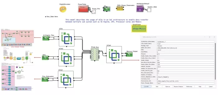
This model describes the usage of UCIe in an SoC architecture to enable data transfer between multiple sub system such as AI Engine, GPU, Processor cores and Memory ScriptTracer Script Tracer
Availability:
VisualSim 3D Modeling IP is available immediately and works with VisualSim Architect 2420 version. The solution runs on Windows, Mac OS and Linux and requires Java 17. The 3D Chiplet library contains configurable UCIe blocks with parameters for clock speed, length and power. The library component can be integrated with chiplets that have PCIe6, AMBA AXI, AMBA CHI, CMN600/700, Tilelink and other interfaces. 10 templates are shipped for direct connect, hub-based, and application partitioning across accelerators, RISC-V, ARM, GPU, NPU, IO and Memory.
About Mirabilis Design Inc:
Leading the march to innovation, Mirabilis Design Inc. integrates requirements to sustainability into the product development flow for semiconductors to networks and systems to software. We partner closely with IP and semiconductor providers to provide accurate System-Level IP for rapid system prototyping and architecture trade-offs. This functional, performance, power, failure, and efficiency analysis reduce the time-to-market, eliminates all surprises prior to development, and enables collaboration between design groups. Learn more at www.mirabilisdesign.com.
Related Chiplet
- DPIQ Tx PICs
- IMDD Tx PICs
- Near-Packaged Optics (NPO) Chiplet Solution
- High Performance Droplet
- Interconnect Chiplet
Related News
- Alphawave Semi Delivers Cutting-Edge UCIe™ Chiplet IP on TSMC 3DFabric® Platform
- Alphawave Semi Taped-Out Industry Leading 64Gbps UCIe™ IP on TSMC 3nm for the IP Ecosystem, Unleashing Next Generation of AI Chiplet Connectivity
- GUC Taped Out UCIe 32G IP using TSMC's 3nm and CoWoS Technology
- Alphawave Semi Launches Industry’s First 3nm UCIe IP with TSMC CoWoS Packaging
Latest News
- NIST Researchers Develop Photonic Chip Packaging That Can Withstand Extreme Environments
- Rebellions Closes $400 Million Pre-IPO and Launches RebelRack™ and RebelPOD™ to Accelerate Global Expansion
- EdgeCortix Looks To Chiplets For Third-Gen Reconfigurable AI Chip
- Agileo Automation Launches Agil'EDA to Accelerate SEMI EDA Adoption for Semiconductor Equipment OEMs
- AEM and ASE Enter Strategic Partnership to Accelerate AI and HPC Test Innovation