ASE Unveils IDE 2.0 – AI-Enhanced Platform Accelerates Package Design Accuracy and Innovation
SUNNYVALE, Calif.-- November 4, 2025 --Advanced Semiconductor Engineering, Inc. (ASE), a member of ASE Technology Holding Co., Ltd. (NYSE: ASX, TAIEX: 3711), today announced the launch of IDE 2.0, a major upgrade to its Integrated Design Ecosystem™ (IDE) platform. The enhanced platform integrates artificial intelligence (AI) to enable faster design iterations, optimize chip-package interaction (CPI) analysis, and accelerate time-to-market for complex AI and high-performance computing (HPC) applications.
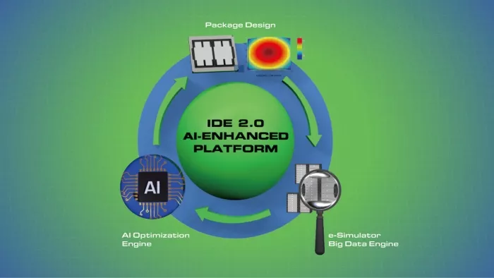
Through its new cloud-based e-Simulator, ASE's IDE 2.0 leverages AI engines to perform CPI predictive risk assessments and optimize design, analysis, and manufacturing data. As advanced packaging continues to play a pivotal role in semiconductor innovation, IDE 2.0 delivers a step-change in efficiency – reducing design cycles and enabling unprecedented precision, performance, and streamlined workflows for ASE's customers.
Building on the proven foundation of its first-generation IDE, ASE's IDE 2.0 represents a transformative advance in advanced package co-design. It introduces an AI-driven feedback framework that continuously connects design and analysis in real time. This intelligent loop enables design teams to innovate faster while managing increasing architectural complexity across multi-die, chiplet, and heterogeneous integration technologies. By combining multiphysics-based simulation, real-world data, and AI insights, IDE 2.0 dramatically improves speed, precision, and reliability in semiconductor package development – empowering customers to make smarter, data-driven design decisions.
At its core, IDE 2.0 accelerates design cycles and enhances risk prediction. The IDE 2.0 workflow provides customers with deeper risk analysis and actionable design insights while safeguarding intellectual property. It enables rapid evaluation of multiple package configurations across mechanical, electrical, and thermal domains – shortening the design-analysis cycle from weeks to hours and ensuring faster, safer, and more effective product launches. With instant risk assessment (RA) analysis, customers can accelerate development, innovate more intelligently, and achieve faster time-to-market where speed is critical.
The ASE IDE 2.0 workflow can dramatically reduce overall design-analysis cycle time from weeks to hours. Key performance highlights include:
- Simulation acceleration: Reduces design iteration time by more than 90%, cutting a 14-day process to just 30 minutes within defined design parameters.
- Integrated multiphysics simulations: Enhances accuracy across electrical, thermal, warpage/stress, and reliability domains.
- AI-based risk prediction: Generates predictive assessments within 60 seconds, enabling real-time design optimization.
"By integrating characterized material and simulation databases with AI-driven capabilities, IDE 2.0 delivers precise insights into chip-package interaction and residual stress," said Dr. C.P. Hung, Vice President of Corporate Research & Development, ASE. "Customers can rapidly model, customize, and optimize designs – reducing prototypes, costs, and time-to-market while protecting IP. It's a major leap forward for packaging architects innovating in the AI era."
"As the world's leading OSAT, ASE continues to innovate relentlessly for its customers," added Yin Chang, Executive Vice President, ASE. "The evolution from automated IDE 1.0 to intelligent IDE 2.0 demonstrates the power of AI in advancing ASE's integrated design ecosystem. As packaging architectures grow more complex, IDE 2.0 enables significant gains in efficiency, quality, and design effectiveness while moving us closer to realizing the Digital Twins vision."
ASE IDE 2.0 is part of VIPack™, ASE's scalable advanced packaging platform aligned with future technology roadmaps. IDE 2.0 is available now as an exclusive collaborative design toolset for ASE customers.
About ASE, Inc.
ASE, Inc. is the leading global provider of semiconductor manufacturing services in assembly and test. Alongside a broad portfolio of established assembly and test technologies, ASE is also delivering innovative VIPack™, advanced packaging, and system-in-package solutions to meet growth momentum across a broad range of end markets, including AI, Automotive, 5G, High-Performance Computing, and more. To learn about our advances in SiP, Fanout, MEMS & Sensor, Flip Chip, and 2.5D, 3D & TSV technologies, all ultimately geared towards applications to improve lifestyle and efficiency, please visit: aseglobal.com or follow us on LinkedIn & X: @aseglobal.
Related Chiplet
- DPIQ Tx PICs
- IMDD Tx PICs
- Near-Packaged Optics (NPO) Chiplet Solution
- High Performance Droplet
- Interconnect Chiplet
Related News
- Chip Assembler ASE Sees Advanced Packaging Sales Doubling
- ISE Labs Investment Secures the Establishment of New Site for Semiconductor Packaging and Test in Mexico
- ASE Expands its Chip Packaging and Testing Facility to Enable Next-Gen Applications
- Diamond Quanta Announces Adamantine Thermal™, Extending Its Advanced Packaging Roadmap Following CES 2026
Latest News
- NIST Researchers Develop Photonic Chip Packaging That Can Withstand Extreme Environments
- Rebellions Closes $400 Million Pre-IPO and Launches RebelRack™ and RebelPOD™ to Accelerate Global Expansion
- EdgeCortix Looks To Chiplets For Third-Gen Reconfigurable AI Chip
- Agileo Automation Launches Agil'EDA to Accelerate SEMI EDA Adoption for Semiconductor Equipment OEMs
- AEM and ASE Enter Strategic Partnership to Accelerate AI and HPC Test Innovation