TSMC looks to standardise chiplet protocols in "world changing" move
By Nick Flaherty, eeNews Europe (October 9, 2023)
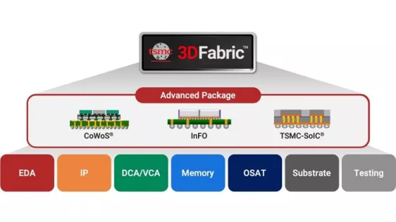
TSMC is looking to develop a standard data format for chiplet designs that would be used by all the EDA design tool and assembly and test providers.
This is part of a move to the 3D Blox technology for building chiplet designs on the TSMC CoWoS process. The aim is to provide common data for chiplets from different silicon suppliers, substrate and PCB makers and the OSAT assembly and test companies.
“Today most of the chips except for the memories come from TSMC but the goal is to mix and match but that is still some way to go but we are trying to get there,” said Dan Kochpatcharin, head of Design Infrastructure at TSMC.
To read the full article, click here
Related Chiplet
- eFPGA Chiplet
- DPIQ Tx PICs
- IMDD Tx PICs
- Near-Packaged Optics (NPO) Chiplet Solution
- High Performance Droplet
Related News
- Alphawave Semi Taped-Out Industry Leading 64Gbps UCIe™ IP on TSMC 3nm for the IP Ecosystem, Unleashing Next Generation of AI Chiplet Connectivity
- Alphawave Semi Delivers Cutting-Edge UCIe™ Chiplet IP on TSMC 3DFabric® Platform
- Strategic alignment between imec and Japan’s ASRA aims to harmonize standardization of automotive chiplet architectures
- Socionext Announces Collaboration with Arm and TSMC on 2nm Multi-Core Leading CPU Chiplet Development
Latest News
- As AI Moves from Training to Inference, Optics Moves Closer to the Chip
- Arteris Announces Collaboration with IC-Link by imec to Accelerate Next-Gen AI and HPC Silicon
- Asahi Kasei Adds New Slitting Facility for SUNFORT™ to Meet Growing Demand for Advanced Semiconductor Packaging
- ACCM Introduces Celeritas SMC: A Production-Ready, Silicon-Matched Core for Advanced Packaging
- Socionext Addresses Datacenter Infrastructure Customer Demands for Advanced SoCs on TSMC A14 Technology