Sony and imec unveil high-density backside connectivity module enabling next-generation 3D chip integration
The new integration approach implements sub-100nm self-aligned through-Si via connections, enabling low-resistance and low-leakage front-to-back connections with good overlay performance
LEUVEN (Belgium), JUNE 16, 2026— This week, at the 2026 IEEE/JSAP Symposium on VLSI Technology and Circuits, imec, a world-leading research and innovation hub in advanced semiconductor technologies, and Sony Semiconductor Solutions Corporation (Sony) jointly present a novel integration module for highly dense backside interconnects – key components of 3D stacking and backside functionalization technologies. The module is structured around a self-aligned local backside dielectric isolation (local BDI) step, resulting in low-resistance and low-leakage highly dense front-to-back through-Si vias (TSVs), with 3x larger overlay window compared to conventional TSV approaches. The local BDI TSV approach is an integration method, which will enable new 3D integration schemes for a variety of use cases, including logic and memory devices.
Backside functionalization and 3D stacking are key enabling technologies for next-generation semiconductor devices. They require high-density backside interconnects to ensure connectivity between the fine-grained active frontside and the less densely structured wafer backside. One attractive approach for making backside interconnects is the via-middle TSV process. While this approach enables high-density front-to-back connectivity, the TSVs typically have a high aspect ratio, which presents challenges in terms of both metallization and electrical performance.
Sony and imec now jointly present an alternative module for integrating backside TSVs, referred to as local BDI. At the heart of this module is a self-aligned isolation structure that is formed locally at the overlap between the TSVs and the active part of the wafer frontside (see also Figure 1). This new approach to backside connectivity has significant advantages over the conventional via-middle TSV process.
Zsolt Tokei, imec fellow and program director of 3D system integration: “Starting from highly dense and narrow via connections already present in the wafer frontside (i.e., the middle-of-line (MOL) vias), our module for the first time allows to transition to much wider TSV connections between the active frontside and the wafer backside. Compared to a via-middle TSV approach, the local BDI TSVs have 50% larger bottom and top critical dimension (CD), simplifying the TSV metallization process and improving its resistance threefold. The process also enlarges the tolerance for misalignment between the TSVs and the narrow MOL vias to up to 30nm – demonstrated for a standard cell configuration with 115nm cell height. In addition, within this improved overlay window, the self-aligned structures provide very good isolation with the surrounding Si substrate as derived from leakage current measurements.”
The process flow starts with conventional FEOL, MOL and BEOL processing, followed by wafer bonding and Si thinning. Local BDI formation at the TSV/active overlap regions consists of conformal dielectric deposition and isotropic etching and is followed by TSV metallization. “The local BDI module will enable new 3D integration schemes for a variety of use cases – including advanced logic and memory applications,” adds Zsolt Tokei. “In addition, as opposed to backside integration schemes that rely on removing the remaining bulk Si, our module allows TSVs to connect through bulk Si with up to 500nm thickness. This is of interest for applications such as DRAM that make use of the relatively thick Si layer remaining at the wafer backside.”
Takushi Shigetoshi, Senior Manager at Sony and lead author of the work adds: "3D integration is becoming increasingly important across a wide range of semiconductor applications, and it is highly meaningful to develop a variety of backside connectivity schemes that can be selected according to the target application."
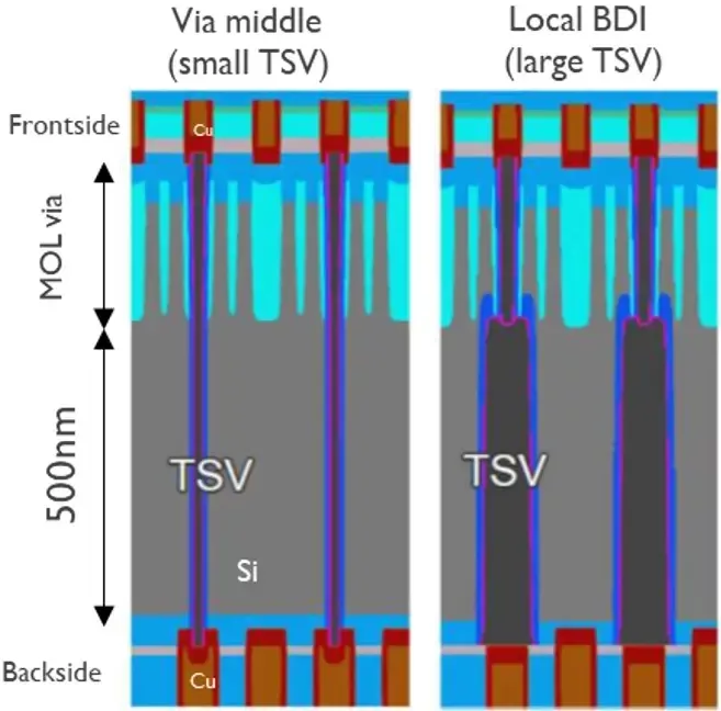
Figure 1 – Schematic comparison of (left) conventional via-middle and (right) local-BDI TSV approaches, assuming a cell height of 115nm and bulk Si thickness of 500nm.
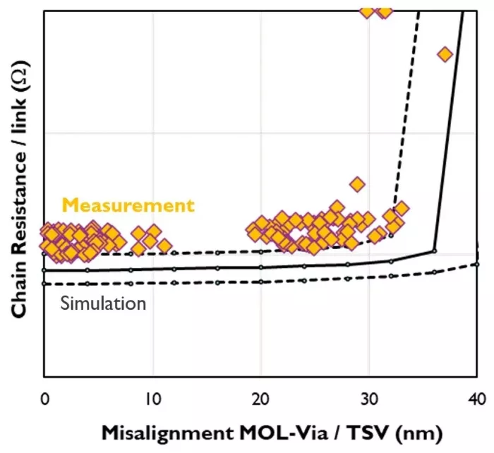
Figure 2 – Overlay dependence of the chain resistance of TSV/MOL-via structures, showing 30nm overlay window. The solid black line represents simulations; dashed lines represent ±5% CD.
About imec
Imec is a world-leading research and innovation hub in advanced semiconductor technologies. Leveraging its state-of-the-art R&D infrastructure and the expertise of over 6,500 employees, imec drives innovation in semiconductor and system scaling, artificial intelligence, silicon photonics, connectivity, and sensing.
Imec’s advanced research powers breakthroughs across a wide range of industries, including computing, health, automotive, industry, consumer electronics, aerospace and security. Through IC-Link, imec delivers customized solutions, from concept to full-scale manufacturing, to meet the most advanced design and production needs. Through imec.ventures, imec creates, co‑creates new ventures, and supports existing semiconductor deep‑tech companies to scale-up.
Imec collaborates with global leaders across the semiconductor value chain, as well as with technology companies, start-ups, academia, and research institutions in Flanders and worldwide. Headquartered in Leuven, Belgium, imec has research facilities in Belgium, across Europe, the USA and the GCC region, and representation on three continents. In 2025, imec reported revenues of €1.2 billion.
For more information, visit www.imec-int.com
Related Chiplet
- Integrated voltage regulator (IVR) chiplet
- High-performance connectivity chiplets
- eFPGA Chiplet
- DPIQ Tx PICs
- IMDD Tx PICs
Related News
- Imec unlocks system-level III-V chiplet integration on Si-CMOS by advancing its 300mm RF silicon interposer platform with high-density MIMCAPs, passive modeling, and laser-assisted bonding
- imec: New Methods for 2.5D and 3D Integration
- Meeting the Cleaning Challenges of High-density 3D Heterogeneous Integration Applications
- The Future of Chip Integration: Fraunhofer IPMS Develops High-Density Chiplet Systems at the Wafer Level
Latest News
- AI Data Centers Push Silicon Photonics Toward 300-mm Scale
- TYLsemi De-Risks Chiplets With New Business Model
- Cadence Introduces AuraStack AI Super Agent, the World’s First Agentic AI Platform for PCB and Advanced Packaging
- Saras Micro Devices Strengthens Senior Leadership Team to Scale Advanced Packaging Technology and Customer Growth
- TYLsemi Raises $43 Million to Launch First Full-Stack Chiplet Platform for Custom AI Silicon