SK hynix unveils ‘iHBM’ thermal solution to boost AI performance
- Enhances heat dissipation by integrating ICEs into the HBM package
- Reduces thermal resistance by 30%, ensuring stable chip operation in demanding high-temperature and high-pressure environments
- Lowers barriers to adoption by leveraging market-proven MR–MUF technology, featuring high design compatibility
Seoul, May 26, 2026 – SK hynix Inc. (or “the company”, www.skhynix.com) announced today the launch of the iHBM solution that embeds integrated cooling elements (ICEs) 1 within the high-bandwidth memory(HBM) package for next-generation HBM products.
Heat management has become a critical challenge as HBM technology advances with higher stacking and faster speeds to cater to the surging demand for AI data processing.
The efficient management of power density 2 in the Die-to-Die Physical Layer (D2D PHY) 3—the interface connecting HBM and GPU—has emerged as a key factor defining the competitiveness of next-generation HBM.
With the iHBM solution, the company has taken a structural approach to addressing the heat management issue. Existing HBM products rely on an indirect cooling method that draws heat away through the core die. In contrast, the iHBM solution places ICEs directly in the D2D PHY area where heat concentration is the highest, creating an additional ‘heat dissipation path’. This latest heat management solution helps reduce thermal resistance by 30% and enables chips to operate stably even in high-temperature and high-pressure conditions.
The company’s mass-production capabilities also serves as a key advantage. SK hynix’s Wafer Level Packaging(WLP) 4 process, based on its market-proven Mass Reflow Molded Underfill(MR-MUF) 5 technology, enables stable high-volume production of iHBM-equipped chips. Furthermore, the solution offers high design compatibility with existing System-in-Package(SiP) 6 architectures, allowing customers to adopt the new thermal technology with minimal design adjustments.
Through the iHBM solution, slated for deployment in next-generation HBM products, including HBM5, SK hynix aims to increase the stability and operational efficiency of HPCs, AI data centers by meeting heat management standards required in high-density and high-bandwidth environments.
“iHBM is an optimal solution for thermal management, combining our memory design capabilities with advanced packaging technology,” said Kangwook Lee, Senior Vice President and Head of PKG Development at SK hynix, adding “The company will cement its AI memory leadership by taking preemptive steps to offer values needed in the AI environment for its customers.”
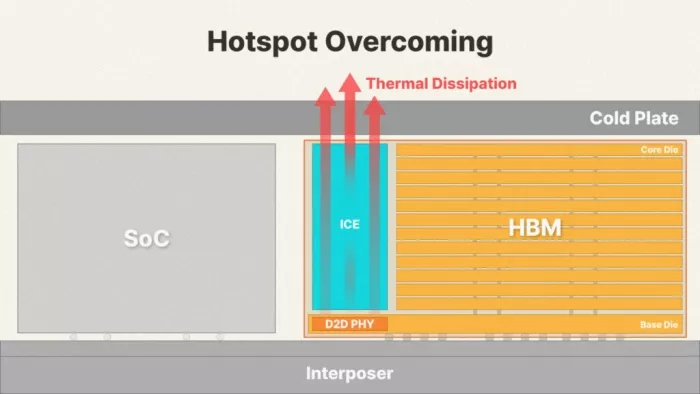
A conceptual diagram of the ‘iHBM Solution’ unveiled by SK hynix
About SK hynix Inc.
SK hynix Inc., headquartered in Korea, is the world’s top-tier semiconductor supplier offering Dynamic Random Access Memory chips (“DRAM”) and flash memory chips (“NAND flash”) for a wide range of distinguished customers globally. The Company’s shares are traded on the Korea Exchange, and the Global Depository shares are listed on the Luxembourg Stock Exchange. Further information about SK hynix is available at www.skhynix.com, news.skhynix.com.
1 ICE(Integrated Cooling Elements): A cooling element made of electrically non-conductive, thermally conductive silicon-based material, designed to dissipate heat from the HBM package by providing an additional thermal path.
2 Power Density: the amount of heat emitting per space serving as a key defining factor for the cooling efficiency and product lifespan.
3 D2D PHY(Die-to-Die Physical Layer): a hardware interface that enables fast data transfer between the HBM base die and AI accelerator.
4 WLP(Wafer Level Packaging): The technology enables the packaging process and testing all at once without cutting a wafer into separate chips. It helps minimize the size of chips and improve electrical efficiency.
5 MR-MUF(Mass Reflow Molded Underfill): A process used for stacking semiconductors by injecting liquid protective materials between chips to protect circuits.
6 SiP(System in Package): A packaging technology that allows different chips to operate cohesively as a one system by placing them next to each other in a vertical or horizontal alignment.
Related Chiplet
- Optical Chiplet
- Reverse Gearbox Chiplet
- FlexGen Multi-Die Smart Network-on-Chip (NoC) IP
- Ncore Multi-Die Interconnect IP
- Integrated voltage regulator (IVR) chiplet
Related News
- SK hynix Signs Investment Agreement of Advanced Chip Packaging with Indiana
- SK hynix Partners with TSMC to Strengthen HBM Technological Leadership
- SK hynix Signs Preliminary Memorandum of Terms with U.S. Department of Commerce for Advanced Packaging Facility in Indiana
- SK hynix Reportedly Plans to Implement Chiplet Technology in Memory Controllers within Three Years
Latest News
- Tenstorrent Releases Open Source Beta of the Open Chiplet Atlas® (OCA) Harness
- Building Out Advanced Packaging Portfolio, JCET Delivers Steady Revenue Growth and Improved Profitability in Q3 YTD 2026
- Egis Group and SiPearl Sign Strategic Cooperation and Investment Agreements to Expand Opportunities on a Global Scale
- Unigen Expands AI Module and Server Compute Collaboration to EdgeCortix RAIDEN Platform
- Amkor Technology and NVIDIA Advance Strategic Partnership for AI Infrastructure