ISSCC 2025: Intel Propels Chiplet Interconnect Speed and Flexibility
The company demonstrated configurable, bandwidth-scalable heterogenous 2.5D interfaces across 20 chiplets from two foundries.
By Duane Benson, All About Circuits (February 25, 2025)
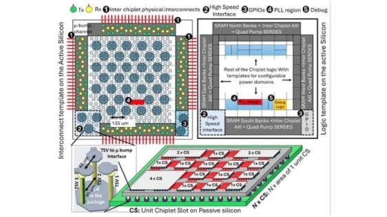
At ISSCC 2025, Intel scientists presented a paper outlining a configurable silicon substrate based on a standard chiplet interface compatible across chiplet types and manufacturers. The paper also proposes a standard interface template for chiplet design with on-chiplet routers for dynamically changing system routing during runtime.
One of the key goals of the new architecture is to remove bandwidth bottlenecks in high-demand AI applications. The proposed solution enhances design flexibility by standardizing the chiplet interface and creating a “mix and match” compatible host for chiplets of various types from different manufacturers.
It also increases operational efficiency and removes bottlenecks by adapting chiplet-to-chiplet routing in real time to bypass unused chiplets. For example, a CPU core not being used in a specific AI inferencing application can be dynamically removed from a pathway between a graphics processing unit (GPU) and a memory chip. This will reduce transfer bottlenecks during data-intensive operations. The CPU code can be routed back in when needed for other operations.
To read the full article, click here
Related Chiplet
- Optical Chiplet
- Reverse Gearbox Chiplet
- FlexGen Multi-Die Smart Network-on-Chip (NoC) IP
- Ncore Multi-Die Interconnect IP
- Integrated voltage regulator (IVR) chiplet
Related News
- Eliyan Showcases Next-Generation Chiplet Interconnect and Memory Innovations at OCP Global Summit 2025
- Keysight Expands Chiplet Interconnect Standards Support in Chiplet PHY Designer 2025
- Brewer Science to Present Temporary Bonding Materials for Chiplet Integration at 2025 Critical Materials Council (CMC) Conference
- Intel Unveils Chiplet Alliance To Enable New Chip Designs
Latest News
- ACM Research Announces Shipment of Its First 310 × 310 mm Ultra ECP ap-p Panel-Level Horizontal Electroplating Production Tool
- Entegris Enters Silicon Carbide and Diamond-Enabled Thermal Management Materials Market for AI Advanced Packaging
- Fraunhofer IPMS Showcases New Technologies for the Future of Semiconductor Industry
- Marvell and Lumentum to Combine, Creating a Category Leader in AI Connectivity
- Silicon Austria Labs Adopts PulseForge Photonic Debonding Technology to Accelerate Advanced Packaging and Heterogeneous Integration Research