Fraunhofer IPMS Showcases New Technologies for the Future of Semiconductor Industry
November 03, 2026 -- At SEMICON Europa 2026, the Fraunhofer Institute for Photonic Microsystems IPMS will showcase current research results and technological developments for the semiconductor industry. The focus is on solutions that open up new ways to integrate diverse technologies, reduce the energy consumption of electronic systems, and enhance the performance of next-generation applications. The portfolio ranges from novel manufacturing and integration approaches to innovative devices and system technologies.
How can different chip technologies be efficiently interconnected? How can memory technologies become more energy-efficient? And what opportunities do photonic technologies create for data processing and sensing? Fraunhofer IPMS will provide answers to these questions at SEMICON Europa 2026 in Munich.
The institute’s exhibition highlights current work from the European pilot lines APECS and FAMES. “Future semiconductor systems will increasingly rely on the interaction of specialized components. The key challenge is to efficiently integrate chiplets, for example with memory or photonic functions, while validating the required processes under industry-relevant conditions. Back-end process technologies are also being introduced into the front-end fabrication of highly complex chips. Together, these advances can enable powerful yet energy-efficient systems,” says Prof. Wenke Weinreich, Director of Fraunhofer IPMS.
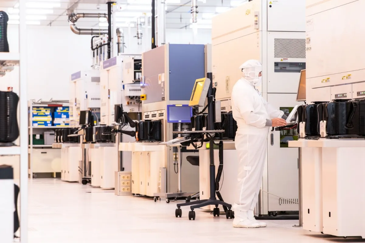
300 mm cleanroom facilities at Fraunhofer IPMS.
APECS Pilot Line: Heterogeneous Integration for Future Semiconductor Systems
APECS stands for Advanced Packaging and Heterogeneous Integration for Electronic Components and Systems. The European pilot line is part of the Chips for Europe Initiative under the EU Chips Act. It is being established under the leadership of the Research Fab Microelectronics Germany (FMD) together with additional European partners.
The goal of APECS is to provide companies with industry-oriented access to advanced packaging and heterogeneous integration technologies. The focus is on integrating different semiconductor components, such as chiplets, memory devices, sensors, and photonic components, into high-performance systems. As a member of the FMD network, Fraunhofer IPMS contributes its expertise in wafer processing, integration technologies, and system development to the pilot line.
At SEMICON Europa, the institute will present current contributions to these technologies.
Interposers and 2.5D Integration
One approach to heterogeneous integration is 2.5D integration. In this concept, multiple chiplets are arranged side by side on a so-called interposer, which is mounted on a substrate similar to a conventional chip. The interposer serves as a high-density interconnection layer between individual components and enables short, high-performance electrical connections.
Functions requiring intensive data exchange, such as sensors and memory devices, can therefore be manufactured separately using different technologies while still achieving data exchange comparable to that of a monolithically integrated chip. This enables computing logic, memory, and specialized functions to be combined in a compact and modular system. Unlike 3D integration, the components are not stacked vertically but positioned side by side on the interposer.
Fraunhofer IPMS develops the necessary process and integration technologies on 200 mm and 300 mm wafers. These activities provide a foundation for scalable chiplet systems and complex heterogeneous system architectures.
Quasi-Monolithic Integration of Chiplets at Wafer Level
With Quasi-Monolithic Integration (QMI), Fraunhofer IPMS is pursuing another approach for high-density chiplet integration. In this process, chiplets are embedded into specially structured recesses, known as pockets, within a silicon wafer. The surface is then planarized and prepared for subsequent wafer-level interconnection.
Within the APECS pilot line, Fraunhofer IPMS has demonstrated for the first time that chiplets can be integrated into a silicon wafer using this method. This achievement marks the first major milestone on the QMI roadmap.
The approach combines the modularity of chiplet-based systems with the high integration density of wafer-based manufacturing. Different chip components can therefore be brought together within a common manufacturing process.
Integrated Platform for the Photonic Systems of the Future
Whether for sensing, data processing, or quantum technologies, integrated photonics provides the foundation for compact and high-performance systems. Fraunhofer IPMS develops electro-optical devices and associated CMOS-compatible manufacturing technologies on 200 mm and 300 mm wafers.
A key technology platform is the institute’s silicon nitride (SiN) waveguide platform, available for both wafer sizes. It features extremely low optical losses across a broad wavelength range, from the visible spectrum to the mid-infrared region, enabling the realization of complex photonic integrated circuits.
This platform serves as the basis for highly sensitive photonic biosensors as well as applications in photonic computing, quantum technologies, and hybrid integration with active components. Electronic and optical functionalities are integrated at wafer level, allowing the resulting devices to be manufactured cost-effectively in large volumes.
Ferroelectric Memories for Fast and Energy-Efficient Electronics
Building on many years of research, Fraunhofer IPMS offers ferroelectric memory technologies based on hafnium oxide as part of its pilot-line services for energy-efficient microelectronic systems.
The technology portfolio includes non-volatile FRAM and FeFET technologies, including reference designs for embedded memories and AI accelerator circuits. Current activities focus on advancing device concepts and process modules and integrating them into established semiconductor manufacturing processes.
These memory technologies operate at voltages below one volt and achieve switching times in the nanosecond range. They combine non-volatile data storage with high endurance and reliability. Specially developed ferroelectric layer stacks from Fraunhofer IPMS help ensure device performance and stability even under demanding operating conditions, such as elevated temperatures.
As a result, these technologies are particularly suitable for embedded applications, intelligent sensor systems, and energy-efficient edge-computing solutions where fast data processing, low power consumption, and permanent data storage are required in highly space-constrained applications.
External partners and customers gain access to the technology platforms, including access to design kits and platform technologies. They can implement their own circuit designs and test structures, have them fabricated, and evaluate them for application-specific solutions or demonstrators. Fraunhofer IPMS provides support from design adaptation and manufacturing through to electrical characterization of the devices.
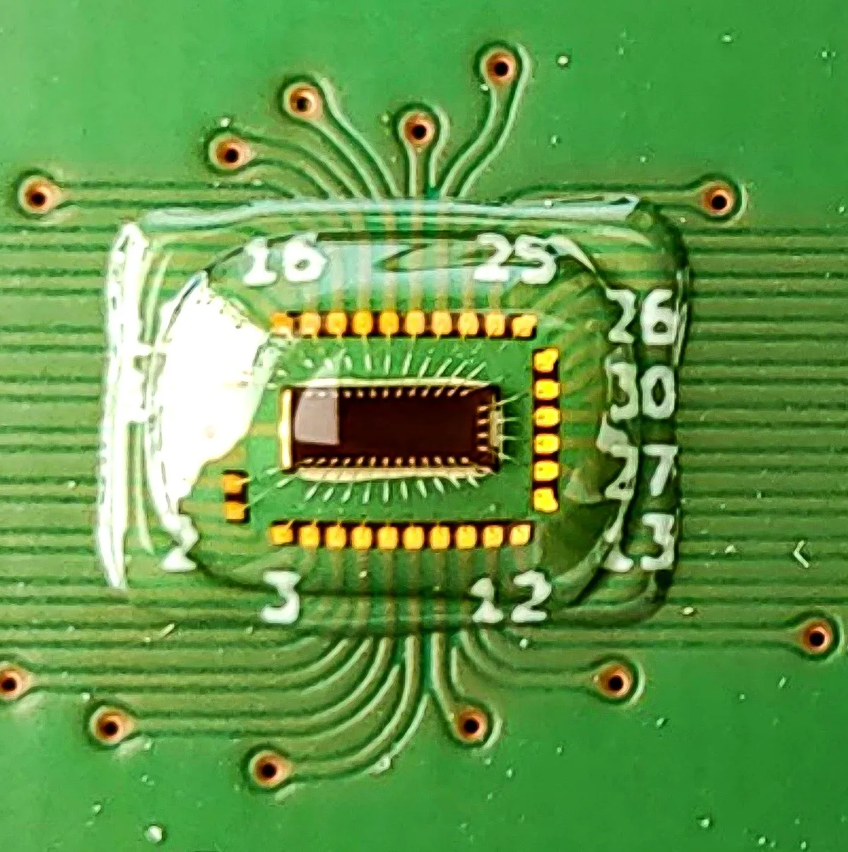
8kbit FeMFET Memory Demonstrator as chip-on board solution developed by Fraunhofer IPMS.
Fraunhofer IPMS at SEMICON Europa 2026
The presented work demonstrates the broad range of technology and manufacturing expertise available at Fraunhofer IPMS, spanning the development of new materials and devices, manufacturing processes on 200 mm and 300 mm wafers, and the integration of complex heterogeneous systems.
“For Europe to maintain a competitive microelectronics industry, new technologies must be successfully transferred from research into industrial application. Reliable process chains and opportunities for industry-oriented validation are essential for this,” concludes Prof. Weinreich.
Fraunhofer IPMS will exhibit at SEMICON Europa in Munich from November 10 to 13, 2026, in Hall B1 at the joint booth with Silicon Saxony, B1 221.
Visitors interested in learning more about Fraunhofer IPMS at SEMICON Europa can arrange a personal meeting at the exhibition booth in advance via the institute’s website.
About Fraunhofer IPMS
Fraunhofer IPMS is a world-renowned research and development service provider specializing in electronic and photonic microsystems. Our technologies are used in industries such as mobility, biotechnology, and medical technology. We are also addressing key future fields, such as quantum technologies and neuromorphic computing. Through our research in green microelectronics, we contribute to a sustainable and resource-efficient world.
At SEMICON Europa 2026, Fraunhofer IPMS will combine its expertise with that of its partners CEASAX and the Research Fab Microelectronics Germany (FMD). Together, the partners cover the entire value chain, from applied research and pilot manufacturing to the scaling of industrial processes. This collaboration enables customers to shorten innovation cycles and bring new technologies into series production more quickly.
Related Chiplet
- Optical Chiplet
- Reverse Gearbox Chiplet
- FlexGen Multi-Die Smart Network-on-Chip (NoC) IP
- Ncore Multi-Die Interconnect IP
- Integrated voltage regulator (IVR) chiplet
Related News
- “From Lab to Fab” – Innovative front-end and advanced packaging technologies for the semiconductor value chain
- Catching Up on The Latest in Advanced Packaging at SEMICON Europa 2024
- European Chiplet Innovation: APECS Pilot Line starts Operation in the Framework of the EU Chips Act
- EV Group Highlights Hybrid and Fusion Bonding, Layer Transfer and Maskless Lithography Technologies for Advanced Semiconductor Memory and Packaging at SEMICON Korea 2026
Latest News
- ACM Research Announces Shipment of Its First 310 × 310 mm Ultra ECP ap-p Panel-Level Horizontal Electroplating Production Tool
- Entegris Enters Silicon Carbide and Diamond-Enabled Thermal Management Materials Market for AI Advanced Packaging
- Fraunhofer IPMS Showcases New Technologies for the Future of Semiconductor Industry
- Marvell and Lumentum to Combine, Creating a Category Leader in AI Connectivity
- Silicon Austria Labs Adopts PulseForge Photonic Debonding Technology to Accelerate Advanced Packaging and Heterogeneous Integration Research