Innolux's Deployment of Key FOPLP Technologies: Leading Next-Gen Advanced Packaging and Seizing AI Opportunities
Advancing Chip-Last and HIPoS integration while delivering one-stop Chip-First panel testing services
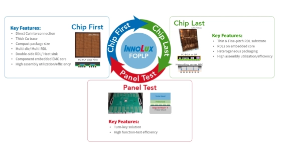 October 16, 2026 -- Miaoli, Taiwan -- Driven by the rapid growth of AI, high-performance computing (HPC), and automotive electronics, chips are evolving toward high performance, chiplet designs, and heterogeneous integration architectures, fueling continuous demand for advanced packaging. According to Counterpoint Research, the global market size for Fan-Out Panel-Level Packaging (FOPLP) and glass substrates packaging is expected to grow from approximately US$650 million in 2024 to over US$8 billion in 2030. Capitalizing on its expertise in large-size panel manufacturing, precision processing, and mass production, Innolux has unveiled its key Chip-Last technology platform, building on its established Chip-First and TGV initiatives. Furthermore, powered by its Heterogeneous Integration Panel on Substrate (HIPoS) platform and one-stop panel testing solution, Innolux achieves rapid, seamless mass production.
As Innolux Chairman and CEO Jim Hung stated, “Integrating large-size panels with advanced packaging enhances material utilization and output per unit, mitigating the cost pressures associated with expanding AI/HPC chip sizes. Moving forward, we will actively pursue customer qualifications and ramp up mass production, collaborating with ecosystem partners to broaden high-value applications across AI, HPC, optical communications, robotics, and automotive electronics, thus contributing to the growth of Taiwan’s semiconductor and advanced packaging industries.”
Successfully developed Chip-Last and HIPoS platform, seizing opportunities of AI and HPC
Innolux unveiled its Chip-Last technology platform, anchored by its HIPoS architecture. By pairing a multi-layer redistribution layer (RDL) with an embedded core structure, this platform delivers scalable advanced packaging solutions, further solidifying Innolux’s strategic footprint in the AI and HPC markets. In the next phase, Innolux will actively promote customer qualification, and is expected to put the technology into mass production in the second half of 2027, actively entering the next-gen advanced packaging supply chain for AI, HPC, and other technologies.
To accelerate the development and production of FOPLP, Innolux has adopted the industry’s largest panel size of 620x670 mm, supporting panel-level packaging with multi-layer RDL and the CoPoS-L like advanced packaging platform. Such large-size panel significantly improves material utilization and output per unit area, effectively easing the cost pressure of expanding AI/HPC chip sizes. Additionally, it provides minimum line/space capabilities down to 2/2 μm to satisfy increasingly complex chiplet integration requirements.
Chip-First's one-stop panel testing solution: Optimizing packaging and testing performance for mass production
In addition to advanced packaging technology, Innolux has also developed a dedicated panel testing solution for Chip-First processes. This solution features a proven mass-production track record, supporting the simultaneous testing of up to 64 chips. By reducing probe movement and index time, it boosts testing efficiency by 50% to 80%, effectively lowering both testing costs and equipment investment requirements. At the same time, combining robust ESD protection mechanisms with multi-temperature zone testing capabilities ensures test stability and quality, while maintaining high mass-production yields.
In addition, Innolux leverages its existing TFT fabs to establish high-spec, move-in-ready production lines, enabling customers to significantly shorten setup times and accelerate time-to-market. Moreover, it provides one-stop vertically integrated services from wafer chip probing and assembly to final testing, connecting testing and packaging processes, optimizing supply chain processes, and improving overall production efficiency and cost-effectiveness.
Innolux is advancing its dual-track transformation, strengthening its advanced packaging expertise. While capturing niche market opportunities, Innolux fully supports the capacity and mass-production demands across diverse AI and HPC applications.
Related Chiplet
- Optical Chiplet
- Reverse Gearbox Chiplet
- FlexGen Multi-Die Smart Network-on-Chip (NoC) IP
- Ncore Multi-Die Interconnect IP
- Integrated voltage regulator (IVR) chiplet
Related News
- Intel’s Embarrassment of Riches: Advanced Packaging
- Onshoring Advanced Packaging Update
- Global Semiconductor IDM Qualifies Veeco Wet Processing Platform for Two New Applications in Advanced Packaging
- Siemens and Intel Foundry advance their collaboration to enable cutting-edge integrated circuits and advanced packaging solutions for 2D and 3D IC
Latest News
- Innolux's Deployment of Key FOPLP Technologies: Leading Next-Gen Advanced Packaging and Seizing AI Opportunities
- Wiwynn, Ayar Labs, and GUC Advance Co-Packaged Optics with Live Demonstration of Integrated Optical Compute System at OCP Global Summit 2026
- ForwardEdge ASIC Announces UCIe 3.0 IP Solution to Accelerate Next-Generation Chiplet-Based ASIC Innovation
- Eliyan Introduces NuLight™: World’s First 2D microVCSEL Interconnect Solution to the Copper Wall
- Evatec delivers first CLUSTERLINE® 310 for Advanced Packaging on small panel formats