Imec advances scalable superconducting technology with world-first NbTiN circuits and 30nm interconnects
New superconducting digital program brings together foundries, system companies and hyperscalers around industry needs in next-gen HPC, AI, quantum computing, photonics and neuromorphic computing
LEUVEN (Belgium), SEPTEMBER 7, 2026— This week, at the 2026 Applied Superconductivity Conference (ASC), imec, a world-leading R&D center in advanced semiconductor technologies, presents a three-metal-level (3ML) niobium-titanium-nitride (NbTiN)-based Josephson junction circuit, achieving circuit design densities of 3.8 million junctions per cm2 – a world first. In addition, 3ML NbTiN routing was demonstrated with superconducting wires scaled down to an unprecedented 30nm linewidth. These results strengthen imec’s versatile NbTiN-based superconducting technology research platform for next-gen HPC and AI applications available for joint R&D with industry partners. Imec’s superconducting digital program is structured around CMOS-compatible process technology, design, and 2.5D and 3D heterogeneous integration. Along with HPC and AI applications, the program also envisions applications in quantum compute control logic, photonics and neuromorphic computing.
Superconducting technology promises to address the expanding needs of high-performance computing (HPC) and AI computational accelerators. It has the potential to significantly outperform state-of-the-art CMOS technology in terms of energy efficiency (100x), compute density (1,000x), and broadcast bandwidth (1,000x). At the device frontend, superconducting technology takes advantage of the fast and low-energy logic offered by Josephson junction circuits. At the backend, superconducting interconnects provide zero-electrical resistance, allowing data to be moved around at extremely low energy and signal losses.
Conventional niobium (Nb)-based superconducting technology, however, lacks the scalability that is required to fully unlock the technology’s potential and open doors to other application domains. Imec addresses the scalability issue with a versatile NbTiN-based superconducting technology research platform that relies on 300mm CMOS-compatible processes. Developments target the co-optimization of technologies and processes, devices, integrated circuits, as well as architecture and system-level metrics.
At 2026 ASC, imec presents NbTiN/αSi/NbTiN-based Josephson junction circuits up to three metal levels (MLs). Junction diameters as small as 150nm are achieved, enabling circuit design densities of 3.8 million junctions per cm2. In addition, three layers of high-density and low-loss NbTiN routing (wires and vias) are demonstrated, which can be used for incorporating inductors, passive transmission lines, ground planes, and clock or power resonators. The NbTiN metal wires were scaled down to 30nm linewidth, which is about 10x smaller than what can be achieved with conventional Nb-based technology. For both Josephson junction circuits and interconnects, the superconducting properties (i.e., critical current density (Jc) and critical current (Ic), respectively) can be controllably tuned to address a broad range of target applications.
Richard Rouse, Director Superconducting Digital Program at imec: “With our superconducting digital program, we are targeting foundries, hyperscalers and system companies to take our NbTiN superconducting technology to the next level. We have structured our program around three pillars: (1) process technology, (2) design and EDA enablement, and (3) system-level scaling centered around 2.5D and 3D integration addressing the co-integration of superconducting devices with other technologies. This heterogeneous approach opens opportunities beyond HPC and AI, including quantum control and readout, neuromorphic computing, and high-resolution single photon detection supporting e.g. space and biomedical applications.”
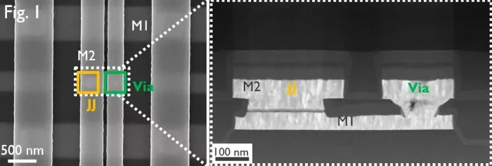
Figure 1 - TDSEM and TEM image of a 2ML αSi-NbTiN Josephson junction.
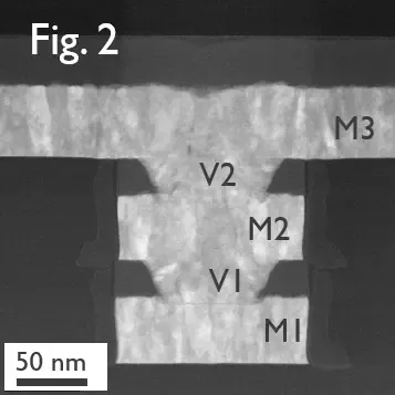
Figure 2 - TEM image of a 3ML NbTiN wires and vias.
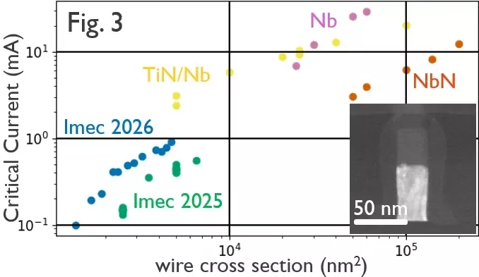
Figure 3 - Wire scaling benchmarking between NbTiN wires fabricated at imec with state-of-the-art superconducting wires. TEM image of a 50nm thick and 30nm wide NbTiN wire (inset).
Related Chiplet
- Optical Chiplet
- Reverse Gearbox Chiplet
- FlexGen Multi-Die Smart Network-on-Chip (NoC) IP
- Ncore Multi-Die Interconnect IP
- Integrated voltage regulator (IVR) chiplet
Related News
- How do UCIe and BoW interconnects support generative AI on chiplets?
- How can in-package optical interconnects enhance chiplet generative AI performance?
- How does UCIe on chiplets enable optical interconnects in data centers?
- NTT looks to 15Tbit/s chiplet optical interconnects
Latest News
- Tenstorrent Releases Open Source Beta of the Open Chiplet Atlas® (OCA) Harness
- Building Out Advanced Packaging Portfolio, JCET Delivers Steady Revenue Growth and Improved Profitability in Q3 YTD 2026
- Egis Group and SiPearl Sign Strategic Cooperation and Investment Agreements to Expand Opportunities on a Global Scale
- Unigen Expands AI Module and Server Compute Collaboration to EdgeCortix RAIDEN Platform
- Amkor Technology and NVIDIA Advance Strategic Partnership for AI Infrastructure