Micron marks first tool move-in at Singapore HBM advanced packaging facility
November 19, 2026 -- Micron Technology, Inc. today celebrated the first tool move-in at its high-bandwidth memory (HBM) advanced packaging facility in Singapore, installing the first process tool into one of its cleanrooms. The milestone follows the successful completion of the critical infrastructure needed for tools installation and marks a significant step toward initial output.
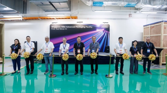 At the ceremony, Micron leaders were joined by Png Cheong Boon, Chairman of the Singapore Economic Development Board, together with representatives from JTC Corporation and ecosystem partners. Chen Kok Sing, senior vice president of Global Assembly and Test at Micron Technology, said, “Construction of our HBM advanced packaging facility is progressing well with initial output expected in early calendar 2027. This milestone reflects the strong execution by our teams and the close collaboration with the Singapore Economic Development Board, JTC Corporation and ecosystem partners. This facility will strengthen our global assembly and test network, reinforcing our commitment to advancing memory and storage technologies that will power the future of AI. We are committed to driving innovation, strengthening the semiconductor ecosystem and enabling the AI era."
Micron broke ground on its HBM advanced packaging facility in Singapore in January 2025, representing an investment of approximately US$7 billion (approximately SG$9 billion) through the end of the decade and beyond. In January 2026, Micron also broke ground on its advanced wafer fabrication facility which will become an integral part of its NAND Center of Excellence, with wafer output expected in the second half of calendar 2028.
The HBM advanced packaging facility will initially create around 1,400 jobs. Together with the advanced wafer fabrication facility, this will bring the total to about 3,000 new jobs, adding to Micron’s more than 10,000 team members in Singapore. As AI drives demand for both memory and storage, Micron expects synergies across its NAND and HBM operations and R&D capabilities in Singapore.
Related Chiplet
- Optical Chiplet
- Reverse Gearbox Chiplet
- FlexGen Multi-Die Smart Network-on-Chip (NoC) IP
- Ncore Multi-Die Interconnect IP
- Integrated voltage regulator (IVR) chiplet
Related News
- Amkor Announces New Site for U.S. Semiconductor Advanced Packaging and Test Facility
- Asahi Kasei Adds New Slitting Facility for SUNFORT™ to Meet Growing Demand for Advanced Semiconductor Packaging
- Veeco Announces Over $35 Million in Advanced Packaging Lithography System Orders From IDM & OSAT Customers
- GlobalFoundries partners with A*STAR to accelerate advanced packaging innovation
Latest News
- Micron marks first tool move-in at Singapore HBM advanced packaging facility
- Microsoft Selects Intel EMIB Packaging for Future Azure Chips
- NVIDIA Expands Commitments With Supply Chain Partners to Support AI Infrastructure Buildout
- ACM Research Expands U.S. Operations with Oregon R&D and Manufacturing Facility as Part of $100 Million Investment
- HTSI & ficonTEC Strengthen Strategic Partnership to Expand Silicon Photonics Testing Capabilities