From Co-Packaged Optics to Nanolasers: Photonics Moves Inward
CEA-Leti, Scintil Photonics, and NcodiN show how optical interconnects are moving from data center racks toward co-packaged optics and chiplet-level communication.
By Pat Brans, EE Times | July 29, 2026
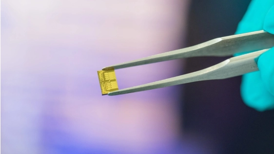
As AI processors become assemblies of GPUs, memory stacks, and specialized chiplets, the optical link is no longer just a data center networking component. It’s becoming part of advanced packaging. CEA-Leti, Scintil Photonics, and NcodiN are each working on a different stage of that transition, from multi-wavelength laser sources for co-packaged optics to nanolasers designed for photonic interposers.
Historically, silicon photonics in data centers has been associated with the front panel of the rack, said Eléonore Hardy, partnership manager at CEA-Leti. Electronics inside the rack perform the computing, while optical transceivers convert electrical signals into photons that can travel through fiber across the data center or beyond.
Hardy said the interconnects now drawing attention are “closer to the chiplets, closer to the GPU, CPU, and memories.” These links are inside the rack, inside advanced packages, and across interposers. Today, many still use copper. But, she said, they are “starting to switch to being also the domain of the photons.”
To read the full article, click here
Related Chiplet
- Optical Chiplet
- Reverse Gearbox Chiplet
- FlexGen Multi-Die Smart Network-on-Chip (NoC) IP
- Ncore Multi-Die Interconnect IP
- Integrated voltage regulator (IVR) chiplet
Related News
- OFC 2025: Scintil Photonics showcases LEAF Light™, world’s first single-chip, multi-wavelength laser source for DWDM co-packaged optics in AI datacenters
- Silicon Photonics and Co-Packaged Optics Shine a Light at OFC 2025
- RANOVUS delivers industry’s first 6.4Tbps Co-Packaged Optics with integrated laser for AI/ML application at OFC 2024
- MediaTek launches next-generation ASIC design platform with co-packaged optics solutions at OFC 2024
Latest News
- Amkor Technology and NVIDIA Advance Strategic Partnership for AI Infrastructure
- Siemens expands agentic AI collaboration to tackle 3D IC power and thermal challenges with NVIDIA
- Photon Bridge Raises €10M to Tackle AI’s Emerging Laser Bottleneck
- Abacus Semiconductor and Aalto University Announce Research Cooperation on High-Speed Chiplet Interconnects
- UK Launches Semiconductor Catapult to Strengthen Sovereign Capabilities in AI Hardware and Defence