Hamamatsu Photonics develops inverted emission microscope "iPHEMOS®-DDX" for failure analysis of advanced semiconductor packages
September 30, 2026 -- Hamamatsu Photonics has developed the iPHEMOS-DDX, an inverted emission microscope designed for failure analysis of advanced semiconductor packages, including AI chiplets, High Bandwidth Memory (HBM), 2.5D/3D packages, and large-scale semiconductor packages. The system enables flexible integration into existing tester-based measurement environments while improving failure analysis workflows and reducing analysis time.
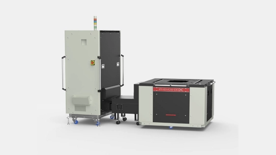 Orders will be accepted starting on September 29, 2026, from semiconductor manufacturers and semiconductor equipment manufacturers worldwide. Hamamatsu Photonics will also exhibit the iPHEMOS-DDX at ISTFA 2026, which will be held in Texas, USA, from October 4 to October 8, 2026.
Background
The semiconductor industry is rapidly advancing with the growth of generative Al, driving increased performance in Al chips while making device structures increasingly complex and highly miniaturized. In particular, advanced semiconductor packages incorporating Al chiplets and High Bandwidth Memory (HBM) achieve high-density integration of multiple chips and memory components, resulting in significantly larger package sizes. As package structures become larger and more complex, identifying failure locations becomes increasingly difficult, creating demand for highly accurate and efficient failure analysis technologies. In addition, advanced semiconductor packages such as Al chiplets are often evaluated under high-speed operating conditions that closely resemble actual operating environments while connected to production testers. Because some failures occur only during high-speed signal transmission, failure analysis technologies capable of accurately capturing abnormal phenomena during operation and identifying failure locations are becoming increasingly important. Additionally, Conventional failure analysis often requires multiple instruments depending on the analysis technique being used. Each instrument change requires sample reinstallation and system reconfiguration. Although systems integrating multiple analysis techniques have become available in recent years, the continued increase in integration density and package size is driving demand for platforms that support a wider range of analysis methods within a single system. Furthermore, semiconductor development laboratories and manufacturing lines are commonly organized around testers, which are generally difficult to relocate once installed.
When facility layouts must be modified to accommodate new products or process changes, tester orientation impose constraints on the placement of surrounding equipment. Because establishing measurement environments and relocating equipment can require significant time and effort, failure analysis systems that can be flexibly installed around existing tester configurations have become an important requirement.
Product overview and expected benefits
The iPHEMOS-DDX is an inverted emission microscope designed for failure analysis of 2.5D/3D packages and large semiconductor packages. Failure analysis of these advanced semiconductor devices requires evaluation under conditions that closely resemble actual operating environments. By directly docking with a production tester, the iPHEMOS-DDX enables analysis under these conditions, making it possible to identify and analyze failure locations and abnormal phenomena that occur only during device operation. Futhermore, the system combines low-drift performance achieved through a low-temperature, high-stability design with seven integrated analysis techniques 1: PEM, Thermal/LIT, LSM, OBIRCH, DALS, EOP/EOFM, and TD Imaging. This enables both static and dynamic failure analysis within a single platform. In addition to emission analysis, the system also supports thermal and laser- based analysis methods. By combining these complementary analytical techniques, it enables failure localization and defect characterization even for challenging failures that cannot be easily identified by emission analysis alone. Furthermore, by consolidating multiple analytical techniques into a single instrument, the iPHEMOS-DDX streamlines failure analysis workflows and helps reduce overall analysis time. The system supports direct docking to testers from three directions, allowing flexible integration into existing Electrical Failure Analysis (EFA) 2 environments.
1: The seven analysis techniques are available across Hamamatsu Photonics’ failure analysis product lineup, with supported techniques varying by model.
- PHEMOS-X: Upright microscope primarily designed for wafer-level emission analysis.
- iPHEMOS-MPX: Inverted microscope supporting emission, thermal, and laser-based analysis of both wafers and packages.
- Dual PHEMOS-X: Integrated platform combining the capabilities of the PHEMOS-X and iPHEMOS-MPX.
- iPHEMOS-DDX: Latest inverted microscope designed for failure analysis of advanced semiconductor devices including Al chiplets and HBM-based packages.
2: Electrical Failure Analysis (EFA) is an analytical process used to identify failure locations in semiconductor devices by detecting physical phenomena such as light emission and heat generation.
Product features
Advanced semiconductor package analysis
Failure locations can be identified while maintaining direct docking to a tester for advanced semiconductor packages utilizing Al chiplets, HBM stacks, interposers, and stacked-die architectures.
Multi-application analysis platform with seven integrated techniques
A platform integrating seven analytical techniques, including PEM, Thermal/LIT, LSM, OBIRCH, DALS, EOP/EOFM, and TD Imaging, enables the entire FA workflow to be performed on a single system.
Flexible docking structure
The system adopts a structure that enables direct docking to a tester from three directions, allowing rapid construction of a tester-centric EFA environment while improving layout flexibility and reducing setup time.
Sales information
- Order start date: September 29, 2026
- Price: USD 1.02 million per system (base configuration, excluding tax) *
- Sales target: 7 systems in Year 1, 9 systems in Year 3, and 10 systems in Year 5
*The listed price is for the base system configuration. Total system price varies depending on the selected configuration. Please contact Hamamatsu Photonics for details.
Related Chiplet
- Optical Chiplet
- Reverse Gearbox Chiplet
- FlexGen Multi-Die Smart Network-on-Chip (NoC) IP
- Ncore Multi-Die Interconnect IP
- Integrated voltage regulator (IVR) chiplet
Related News
- Veeco Announces Multiple Orders for Wet Processing and Lithography Systems to Support Advanced Packaging and Silicon Photonics at a Leading Semiconductor Foundry
- Tokyo Electron and IBM Renew Collaboration for Advanced Semiconductor Technology
- Global Semiconductor IDM Qualifies Veeco Wet Processing Platform for Two New Applications in Advanced Packaging
- Arteris Joins Intel Foundry Accelerator Ecosystem Alliance Program to Support Advanced Semiconductor Designs
Latest News
- Amkor Technology and NVIDIA Advance Strategic Partnership for AI Infrastructure
- Siemens expands agentic AI collaboration to tackle 3D IC power and thermal challenges with NVIDIA
- Photon Bridge Raises €10M to Tackle AI’s Emerging Laser Bottleneck
- Abacus Semiconductor and Aalto University Announce Research Cooperation on High-Speed Chiplet Interconnects
- UK Launches Semiconductor Catapult to Strengthen Sovereign Capabilities in AI Hardware and Defence