AI Drives Larger, Denser Packaging, Raising New Challenges for Equipment Makers
By Susan Hong, EE Times | September 30, 2026
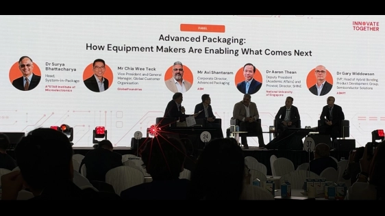
Artificial intelligence is pushing advanced packaging in seemingly opposite directions: Package sizes are getting larger, while interconnect pitches and defect tolerances continue to shrink.
At A*STAR’s Innovate Together 2026 in Singapore, experts from KLA, ASM, ASMPT, and the National University of Singapore (NUS) discussed how advanced packaging is evolving beyond individual equipment or process technologies. The challenge is to integrate materials, bonding, metrology and inspection, optical interconnects, and system design while maintaining yield, reliability, and cost efficiency across larger package areas and finer interconnect pitches.
Surya Bhattacharya, head of system-in-package at A*STAR’s Institute of Microelectronics (IME) and moderator of the panel, said that as continued transistor scaling becomes insufficient to meet AI computing demands, systems must integrate more dies and functions, making packaging an increasingly integral part of system design.
To read the full article, click here
Related Chiplet
- Optical Chiplet
- Reverse Gearbox Chiplet
- FlexGen Multi-Die Smart Network-on-Chip (NoC) IP
- Ncore Multi-Die Interconnect IP
- Integrated voltage regulator (IVR) chiplet
Related News
- Applied Materials Introduces New Systems to Accelerate DRAM and Advanced Packaging for AI Chips
- Onto Innovation’s Dragonfly® G5 System Qualified for Applications in 2.5D AI Packaging
- AI Optical Interconnect Boom Drives U.S. Firms to Expand Southeast Asia Outsourcing, Opening the Door for Cross-Industry Entrants
- JCET Launches Next-Generation Power Module Packaging and Test Solutions for AI Data Centers
Latest News
- Building Out Advanced Packaging Portfolio, JCET Delivers Steady Revenue Growth and Improved Profitability in Q3 YTD 2026
- Egis Group and SiPearl Sign Strategic Cooperation and Investment Agreements to Expand Opportunities on a Global Scale
- Unigen Expands AI Module and Server Compute Collaboration to EdgeCortix RAIDEN Platform
- Amkor Technology and NVIDIA Advance Strategic Partnership for AI Infrastructure
- Siemens expands agentic AI collaboration to tackle 3D IC power and thermal challenges with NVIDIA