Bringing Tiny Chiplets To Embedded SoCs
By Sally Ward-Foxton, EETimes (October 31, 2023)
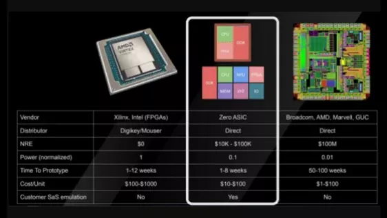
LONDON — ZeroASIC has developed a technology platform to bring chiplets to embedded system design, as a time-efficient alternative to designing and manufacturing custom application-specific ICs (ASICs). The platform is based on swappable pre-fabbed 2 x 2 mm chiplets on an active silicon interposer, which customers can design for themselves in a matter of minutes using ZeroASIC’s online EDA tool.
The company’s aim is to reduce the barrier to making custom ASICs versus using off-the-shelf SoCs. ZeroASIC CEO Andreas Olofsson told EE Times that the biggest cost, in terms of both time and money, for custom ASICs is tapeouts.
To read the full article, click here
Related Chiplet
- DPIQ Tx PICs
- IMDD Tx PICs
- Near-Packaged Optics (NPO) Chiplet Solution
- High Performance Droplet
- Interconnect Chiplet
Related News
- Empower Semiconductor Showcases High-Density Power Chiplets and Embedded Integrated Voltage Regulators at APEC 2024
- Baya Systems Introduces New Technology to Transform SoCs and Chiplets for Emerging Applications
- On chip voltage regulator IP for chiplets and SoCs
- Alphawave Semi to Reveal Ecosystem and Key Architectures Unlocking Generative AI Potential at EE Times' "Chiplets: Building the Future of SoCs" Seminar
Latest News
- GlobalFoundries qualifies SLATE™ advanced packaging technology on 9SW platform for next-generation radio frequency applications
- Qnity Powers the Transition from Shrink to Stack with Advanced Packaging Solutions
- NHanced Semiconductors President Robert Patti to Deliver Plenary Presentation on the Critical Role of Advanced Packaging at the 2026 Lithography Workshop
- Intel Announces Leadership Appointment at Intel Foundry to Accelerate Development and Manufacturing
- HyperLight Announces $80 Million Series C to Accelerate TFLN Deployment for AI Infrastructure