Baya Systems Expands Bengaluru Engineering Hub to Scale AI, Automotive and HPC Innovation
Long-term investment in India accelerates software-driven, chiplet-ready fabric.
Bengaluru – January 15, 2026 -- Baya Systems, a pioneer in software-driven, chiplet-ready semiconductor fabric IP for scalable AI, high-performance computing (HPC) and automotive applications, today announced the opening of its expanded engineering hub in Bengaluru, India, reinforcing the company’s commitment to scaling global engineering capacity as demand for AI infrastructure accelerates.
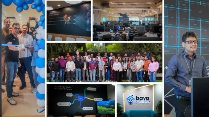
What: In less than two years, Baya Systems’ Bengaluru operation has strengthened into a major global engineering hub, playing a central role in the development and delivery of the company’s software-defined semiconductor fabric technologies that power scalable, high-performance, chiplet-based systems for AI and HPC systems worldwide.
The Bengaluru office, which opened with just five employees in 2023 in conjunction with the inception of Baya Systems, has now expanded to more than 50 engineers, with plans to exceed 100 employees by the end of 2026. The expansion reflects Baya’s strategy to increase execution velocity, deepen cross-site collaboration and accelerate delivery of next-generation fabric IP at scale, while making a sustained investment in India’s innovation hub and its world-class semiconductor and software talent.
When: Wednesday, January 14, 2026
Where: Brigade Metropolis, Bengaluru, India
Why: Global demand for AI, data center and HPC infrastructure is surging, fueled by an increased shift towards chiplet-based, software-defined architectures. India has rapidly become a critical hub for semiconductor design, verification and software engineering. Baya’s extended hub provides immediate access to this deep talent pool to enable faster innovation today and reinforcing the company’s role in the global semiconductor value chain.
Baya Systems’ expansion strategy focuses on growing close to major innovation centers including Cambridge, U.K., where the company recently opened its first European office. This gives Baya proximity to a wide range of talent, diverse ecosystems, and localized customers, accelerating core innovation and product development while further improving its support response.
Related Chiplet
- eFPGA Chiplet
- DPIQ Tx PICs
- IMDD Tx PICs
- Near-Packaged Optics (NPO) Chiplet Solution
- High Performance Droplet
Related News
- Baya Systems Strengthens Engineering Leadership to Accelerate Chiplet Implementation
- Thinking Big: From Chips To Systems
- Baya Systems Introduces New Technology to Transform SoCs and Chiplets for Emerging Applications
- Tenstorrent Licenses Baya Systems’ Fabric into next-generation AI and Compute Chiplet Solutions
Latest News
- As AI Moves from Training to Inference, Optics Moves Closer to the Chip
- Arteris Announces Collaboration with IC-Link by imec to Accelerate Next-Gen AI and HPC Silicon
- Asahi Kasei Adds New Slitting Facility for SUNFORT™ to Meet Growing Demand for Advanced Semiconductor Packaging
- ACCM Introduces Celeritas SMC: A Production-Ready, Silicon-Matched Core for Advanced Packaging
- Socionext Addresses Datacenter Infrastructure Customer Demands for Advanced SoCs on TSMC A14 Technology