When EMC Shielding Must Bend With the Package

Why soft conductive materials must preserve electromagnetic, thermal, mechanical, and reliability performance together
A package engineer replaces a rigid metal shield with a soft conductive film.
The first results look promising.
The film lowers the profile. It follows the board contour. It removes brackets and fasteners. It simplifies assembly. It may even help carry heat away from a local hotspot.
Then the package enters thermal cycling.
The substrate bends. Contact pressure changes. The polymer relaxes. One edge begins to lift. Electrical contact resistance rises. The return current spreads into a longer path. Heat crosses a different interface than the thermal model assumed.
The film may still look intact.
The package may no longer behave the same way.
That is the central challenge.
A soft conductive film is not simply a flexible replacement for a metal shield can. Once it touches the package, it becomes a multifunctional interface. It must shield electromagnetic energy, preserve electrical contact, follow mechanical deformation, support heat transfer, survive environmental stress, and remain manufacturable.
The material creates the opportunity.
The package creates the operating conditions.
Reliability evidence must connect the two.
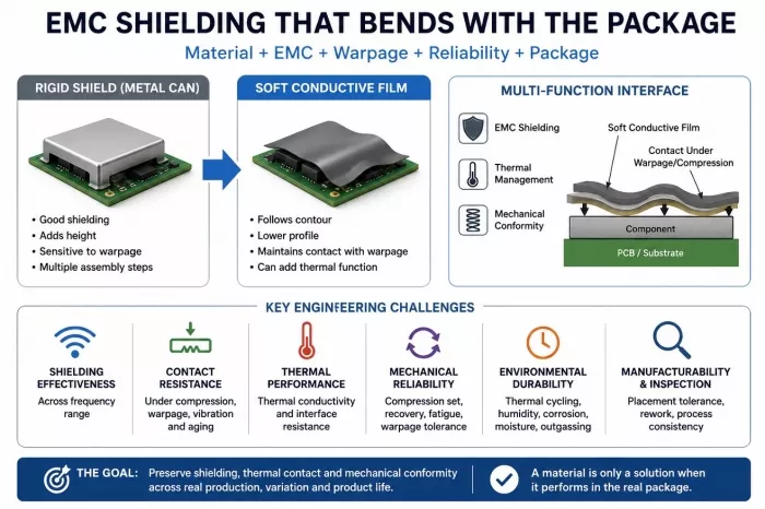
Why rigid shielding is reaching a physical limit
Traditional shield cans work well because they create a defined conductive enclosure around a noisy or sensitive region. Their geometry gives return current a predictable path and helps contain electric and magnetic fields.
But rigid structures consume height and board area.
They require attachment features, grounding locations, seams, clips, solder joints, or fasteners. They may interfere with airflow, cooling hardware, connectors, optical paths, and rework access.
As AI processors, automotive controllers, robotic systems, and densely populated boards place more functions into smaller spaces, the available shielding volume shrinks.
Package and board warpage make the problem harder.
A rigid shield assumes that its attachment points and mating surfaces remain close to their intended positions. A large package, thin board, uneven component field, or repeated thermal cycle can change those positions.
When a shield loses contact at one point, the problem is not merely mechanical.
The gap changes the electromagnetic boundary.
Current may detour around the opening. The larger loop can increase inductance. A seam can behave like an aperture. Fields can leak into a neighboring circuit or cable. The shield remains present, but its electrical function has changed.
A soft conductive film offers a different approach.
Instead of forcing the package to meet one rigid geometry, the shielding layer follows the package.
That sounds simple. It is not.
Conductivity does not prove shielding
A supplier can measure low sheet resistance and show that a film conducts electricity.
That is useful, but it does not prove that the assembled package will meet its EMC requirement.
Shielding effectiveness depends on more than bulk conductivity. It also depends on frequency, thickness, magnetic properties, geometry, grounding, seams, apertures, contact resistance, and the source and victim locations.
Researchers have demonstrated flexible films with strong measured shielding performance after extensive bending. One ultrathin Ni/Ag composite maintained low sheet resistance and more
than 40 dB of shielding around 8 GHz after repeated flexing. Other graphene and polymer structures have shown that very thin, lightweight materials can provide substantial shielding.
Those results prove that flexible shielding materials can work.
They do not prove that every film will work inside a real package.
A laboratory coupon usually has clean surfaces, controlled dimensions, defined fixtures, and uniform contact. A package contains corners, gaps, connectors, fasteners, adhesive boundaries, local pressure differences, surface contamination, and manufacturing tolerances.
The design team must therefore test the complete current path:
noise source → shield surface → grounding contact → package or board return structure
The package does not care whether the film has an impressive conductivity value in isolation.
It cares whether current can reach the correct reference with low and stable impedance.
Warpage turns contact into a moving variable
Two surfaces that appear flat touch only at small microscopic regions.
Pressure increases the true contact area. Surface films, roughness, oxidation, contamination, and mechanical load all influence electrical contact resistance.
A soft film can improve conformity by filling gaps and following uneven surfaces. But its resistance may still change as the package bends, vibrates, heats, cools, or ages.
The engineering team must ask:
- How much compression creates reliable contact?
- How much compression can the film tolerate?
- Does the film recover after the load is removed?
- Does resistance change after thousands of cycles?
- What happens when warpage shifts pressure from the center to the edges?
- Does the conductive network crack, separate, or rearrange under strain?
Flexible conductive composites can show piezoresistive behavior because deformation changes the spacing and contact among conductive particles, fibers, flakes, or metallic layers. Some materials recover after unloading. Others retain hysteresis or accumulate damage.
This means the package needs more than an initial resistance measurement.
It needs a resistance-versus-pressure curve, a resistance-versus-warpage curve, and a resistance-versus-life curve.
A four-wire Kelvin measurement can help isolate the interface resistance from the leads and probes. The team can then monitor the shielding contact while applying controlled compression, curvature, temperature, and vibration.
That creates evidence about the actual interface—not just the raw material.
Thermal performance adds another interface
The opportunity becomes more attractive when the same film can also help move heat.
A multifunctional layer could reduce part count by combining:
- EMC shielding
- electrical grounding
- mechanical conformity
- thermal contact
But thermal performance cannot be inferred from bulk thermal conductivity alone.
Heat must cross two physical interfaces:
hot component → conductive film → spreader, lid, shield, or chassis
Surface roughness and incomplete contact create thermal resistance. Pressure changes the real contact area. Voids trap air. Adhesive layers add another thermal barrier.
Recent research on thermal-interface materials shows that both bulk properties and interfacial thermal resistance can change with mechanical pressure and can display hysteresis during loading and unloading.
This matters when the package warps.
One area may gain contact while another loses it. The average pressure may remain acceptable while the local thermal path degrades above the hottest component.
A datasheet value measured under one pressure cannot answer the full package question.
The design team must measure:
- thermal resistance at realistic compression;
- pressure distribution across the package;
- resistance after thermal cycling;
- performance under warped and flat conditions;
- interaction between the adhesive, conductive layer, and mating surfaces;
- local temperature gradients, not only average temperature.
The film succeeds thermally only when it preserves the complete heat path under the same conditions that challenge its EMC contact.
One material can create competing requirements
The material designer may increase conductive filler to improve shielding.
That change can make the film stiffer.
A stiffer film may follow warpage less effectively.
The team may soften the polymer to improve conformity.
That can increase creep or compression set.
A stronger adhesive may improve assembly.
It can make rework difficult or introduce another electrically resistive layer.
A thicker film may fill larger gaps.
It can increase thermal resistance or require more compression.
A thin metallic coating may lower sheet resistance.
It may crack during bending or corrode under humidity.
These are not separate material-selection problems.
They are coupled package decisions.
The correct question is not:
Which film has the highest conductivity?
It is:
Which material stack preserves shielding, grounding, thermal contact, mechanical recovery, and assembly margin across the product’s life?
Reliability must test the combined function
A conventional qualification plan may test electrical, thermal, and mechanical behavior in separate experiments.
That can miss the important failure path.
Suppose a film passes a bend test.
It may still lose electrical contact after heat and humidity age the surface.
Suppose it passes an initial shielding test.
Its adhesive may creep during prolonged high-temperature operation.
Suppose it transfers heat well under high compression.
The package may not tolerate that load without stressing solder joints, optical alignment, or the board.
A useful reliability sequence should apply realistic stress and then remeasure every important function.
For example:
- Assemble the film using the intended production process.
- Measure initial shielding effectiveness, contact resistance, thermal resistance, and package flatness.
- Apply thermal cycling, humidity, vibration, and sustained compression.
- Measure warpage and pressure distribution again.
- Repeat the electromagnetic, electrical, and thermal measurements.
- Inspect for cracks, delamination, corrosion, particle movement, and adhesive failure.
- Compare the remaining margin with the product requirement.
This sequence matters because a mechanically intact film may have degraded electrically. A stable resistance value may hide a weakened adhesive. A good average thermal result may hide a local gap.
Reliability is not one final test.
It is the evidence that all required functions remain connected after stress.
Manufacturing can decide the winner
Even a technically strong material can fail as a production solution.
The process must control film thickness, placement, compression, surface preparation, grounding area, adhesive cure, overlap, and edge geometry.
Operators or automation must position the material without trapping contamination or creating folds. Inspection must detect incomplete contact, wrinkles, tears, voids, lifted edges, and misplaced sections.
The package team must also decide:
- Can the film be removed without damaging the board?
- Can technicians inspect or replace components beneath it?
- Does it interfere with optical inspection or electrical test?
- Can automated equipment place it at volume?
- How will the factory verify compression?
- Can the process tolerate normal package and board variation?
A material that combines three functions can reduce parts and assembly steps.
It can also combine three failure modes into one layer.
That makes process control more important, not less.
A practical decision point
Before releasing the design, the engineering team should be able to answer five questions.
Does it shield?
The complete assembly meets its emission and immunity targets across the required frequency range.
Does it remain grounded?
Contact resistance stays within margin across warpage, compression, vibration, temperature, and aging.
Does it move heat?
The complete thermal interface maintains acceptable resistance and gradients under realistic pressure.
Does it recover?
The material resists compression set, cracking, creep, delamination, and environmental degradation.
Can the factory control it?
Placement, inspection, rework, and release criteria are clear and repeatable.
Only then can the team decide whether the film is ready.
The package is the real test
Soft conductive shielding could become valuable as packages and boards grow denser, thinner, hotter, and less mechanically uniform.
It can follow contours that rigid metal cannot. It can lower profile. It can simplify assembly. It may combine EMC shielding, thermal contact, and mechanical conformity in one interface.
But the film must earn that role.
A strong coupon result proves material capability.
A stable assembled result proves package readiness.
The difference is evidence.
A soft conductive film is not successful because it bends.
It is successful when shielding, heat transfer, contact, and mechanical conformity continue to work while the package bends around it.
Related Chiplet
- Optical Chiplet
- Reverse Gearbox Chiplet
- FlexGen Multi-Die Smart Network-on-Chip (NoC) IP
- Ncore Multi-Die Interconnect IP
- Integrated voltage regulator (IVR) chiplet
Related Blogs
- When the Package Becomes an Electrical Design Variable
- Addressing the Colossal Challenge of System Co-Optimization with a Holistic Chiplet Design Methodology
- Advancing the Open Chiplet Ecosystem with UCIe 2.0
- UMI: Extending Chiplet Interconnect Standards To Deal With The Memory Wall