Understanding the Difference Between a Monolithic SoC and a Chiplet

I am often asked, "What is the difference between a traditional SoC die and a chiplet die?" At a high level, the answer is that a traditional SoC is designed as a standalone single-die packaged chip, while a chiplet is part of a larger system of multiple dies packaged together. This simple answer inevitably leads to a more involved answer. To facilitate a system of chiplets, each chiplet must understand how to manage itself within the system. One common misconception is that adding a die-to-die interface to a design equals a "chiplet." While that is part of the chiplet function, it is nowhere near solving all the associated challenges.
To operate as a chiplet, a design must first address a number of considerations. These include how it boots (secure or insecure?), how it's debugged (standalone or across chiplets?), how common resources (such as memory) are managed, how clocking and resets are distributed, how it communicates with other chiplets, and, for designs where safety is crucial, how faults are captured. Finally, all these capabilities should be designed to a common specification, such as the new Foundational Chiplet System Architecture (FCSA), being developed as part of the Open Chiplet Economy (OCE), to ensure multi-chiplet interoperability. The FCSA specification defines common interfaces and protocols between different types of chiplets.
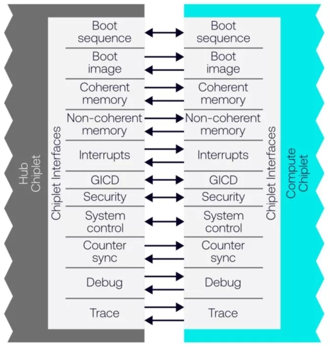
Figure 1. Common Chiplet Interfaces
The Cadence Chiplet Framework
The good news for chiplet designers is that Cadence has been pondering the problems of multi-die chiplet integration and interoperability, and the need for specific chiplet management capabilities, for a couple of years now, and has developed a solution. The Cadence Chiplet Framework is a comprehensive hardware and software solution designed to make this transition seamless. The Cadence Chiplet Framework accelerates chiplet development and ensures cross-chiplet interoperability by standardizing common interfaces.
The Cadence Chiplet Framework provides a pre-verified and integrated set of subsystems that manage everything from boot-up and security to die-to-die communication. It acts as the foundational blueprint for creating complex multi-chiplet systems. Let's explore the key subsystems that compose this powerful framework and understand how each component contributes to a successful chiplet-based design.
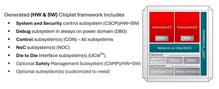
Figure 2. Cadence Chiplet Framework
To read the full article, click here
Related Chiplet
- eFPGA Chiplet
- DPIQ Tx PICs
- IMDD Tx PICs
- Near-Packaged Optics (NPO) Chiplet Solution
- High Performance Droplet
Related Blogs
- Faster, More Collaborative SoC and Chiplet Architecture Exploration: Introducing Synopsys Platform Architect Development Kit (PADK)
- GlobalFoundries, MIPS, and the Chiplet Race for AI Datacenters
- The Growing Chiplet Ecosystem: Collaboration, Innovation, and the Next Wave of UCIe Adoption
- Bosch and the chiplet revolution: Enabling software-defined mobility
Latest Blogs
- How Intel Foundry Packaging Technologies Redefine AI and HPC Scalability Limits at ECTC 2026
- From complexity to simplicity: Scaling and future-proofing chiplets with AMBA®︎ CHI C2C property negotiation
- High-Speed Heterogeneous Integration with Multiphysics Analysis for TSMC SoW-X
- Chiplet Realization Beyond the Package: Why the Next AI Bottleneck Moves to the Interposer-to-PCB Boundary
- Advancing UCIe Performance: Enabling 40G for Next-Generation Multi-Die Designs