Accelerating Next-Generation EMIB-T Packaging: A Collaboration Between Synopsys and Intel Foundry
Introduction
Advanced packaging has quietly become one of the most important forces shaping modern compute systems. As AI and high-performance computing push the limits of what’s physically possible on a single die, the industry has steadily shifted toward multi-die designs. But stitching together multiple dies requiring extremely high bandwidth while maintaining clean power delivery is anything but simple. And this is exactly the challenge Intel Foundry set out to solve with its newest evolution of embedded bridge technology: EMIB-T (Embedded Multi-die Interconnect Bridge-TSV)
EMIB-T represents a major leap forward. It brings together dense chip-to-chip connections, improved signal integrity, and, perhaps most critically, a dramatically enhanced power delivery pathway made possible through TSVs embedded directly in the bridge. Designers need automation. They need predictable flows. They need analysis built-in from the start.
And that’s where the Synopsys story begins.
A New Packaging Challenge Emerges
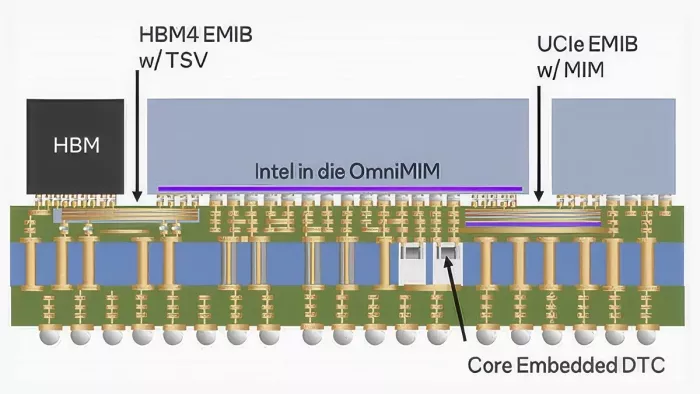
The push toward architectures built around large compute dies, next generation HBM stacks, and broad clusters of AI accelerators created a packaging problem that traditional 2.5D approaches could no longer solve elegantly. Modern systems were demanding enormous package footprints, sometimes reaching 120 mm × 180 mm, and in many cases requiring more than 30 individual EMIB bridges stitched across the substrate.
These systems weren’t just large. They were power hungry, dense, and incredibly sensitive to noise. HBM4 and HBM4e pushed power delivery requirements even higher. Meanwhile, the UCIe interfaces connecting major compute dies began reaching high speeds, with routing rules and signal integrity demands to match.
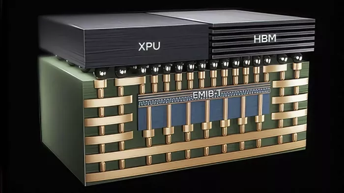
Intel Foundry’s earlier EMIB technology has already proven the value of short-reach silicon bridges. But this next generation required something more. It needed a way to deliver power directly through the bridge, not just signals. It required tighter integration of multiple dies. And it needed a routing architecture ready for a world built on UCIe-based chiplet ecosystems and hungry for memory bandwidth.
Thus, EMIB-T was born, complete with TSV enabled power delivery, backside bumping, denser MIM capacitors, and routing designed specifically for the high-speed protocols that will define the next decade of computing.
Turning EMIB-T Into a Real Design Flow
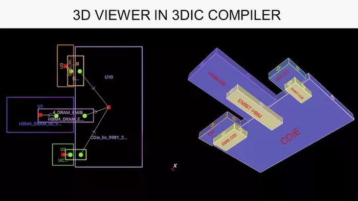
A breakthrough in packaging technology is only half the story. Without an automated, predictable EDA flow, the barrier to adoption becomes too high, even for engineering teams eager to experiment. Intel Foundry understood this, and so our collaboration began: develop a full end-to-end EMIB-T workflow using Synopsys 3DIC Compiler, a unified exploration-to-signoff platform, making the advanced packaging capabilities accessible to any chip designer.
This required deep engineering work on both sides, iteratively refining the design flow, validating design assumptions, building algorithmic automation, and ensuring manufacturability every step of the way.
One of the early challenges involved the very first step of EMIB-T system design: simply defining the bridges. Determining the proper width, height, and placement of each EMIB-T block needs to be done carefully including considerations for silicon package thermal coefficient mismatch. Synopsys and Intel Foundry co-engineered algorithms that could take in chiplet bump maps, analyze the die-to-die interface automatically, and determine exactly how each bridge should be sized and where it must be placed. This approach will scale easily for systems containing dozens of bridges.
That philosophy, reduce friction through automation- became the theme of the entire reference methodology.
Building a Unified, Automated, 3DIC-Aware Flow
From the very beginning, Synopsys and Intel Foundry designed the flow so a user could describe their chiplet system through a standards-based format and immediately bring those models into 3DIC Compiler. From there, the tool takes over much of the heavy lifting.
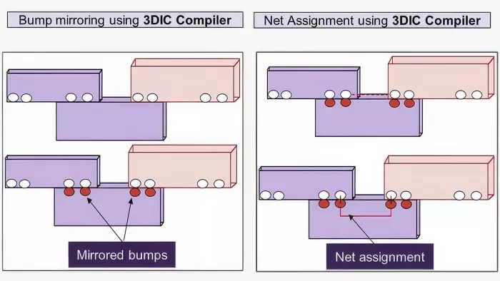
Chiplet bumps are mirrored automatically onto EMIB-T structures. Net assignment, formerly a time-consuming source of human error, is handled algorithmically. High speed routing for both UCIe and HBM using 3DIC Compiler follows Intel Foundry’s PDK specific rules providing a correct-by-construction approach to meet stringent performance requirements, even width constraints or angle limitations. Even intricate power features, such as TSV insertion and backside bump creation, are generated based on the chiplet’s power/current demands.
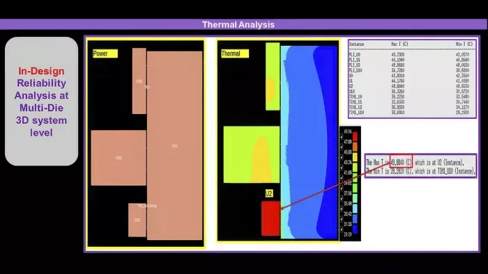
Thermal and IR/EM analysis, traditionally performed late in the cycle, becomes part of design exploration.
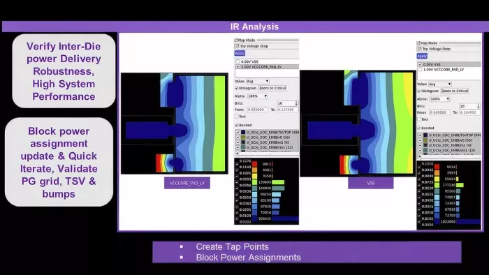
With Synopsys Redhawk-SC and RedHawk-SC Electrothermal running inside 3DIC Compiler, designers can visualize heat generation, heat spread, current density, and voltage droop, long before tapeout. Instead of weeks of exporting and reimporting models between tools, teams can import models between tools and receive instant feedback while still iterating.
By the time signoff checks begin, DRC, LVS, antenna, tape-in validation via Synopsys IC Validator; the flow has already been conditioned to manufacturing rules for EMIB-T. To close the loop, formal verification through Synopsys Formality ensures that once the bridge structures and routing are inserted, the connectivity remains consistent with the original golden netlist.
What This Means for Chip Designers
The real impact of this collaboration is that designers no longer need to piece together fragmented tools or manually interpret complex packaging rules. Synopsys 3DIC Compiler allows for EMIB-T to become accessible and predictable, and for development cycles to shorten dramatically. Power and thermal problems reveal themselves earlier. High bandwidth chiplet integration becomes straightforward. Most importantly, teams gain the confidence to push boundaries, knowing the underlying infrastructure is sound.
Through this work, Intel Foundry’s advanced packaging capabilities open to a broader ecosystem. Whether a developer is integrating massive compute dies, building UCIe-based accelerators, or experimenting with next generation HBM architectures, EMIB-T becomes a viable platform.
Synopsys’ 3DIC Compiler platform becomes the bridge between chip design, advanced packaging, signoff, and system level validation. This unified approach helps usher in a new era of heterogeneous computing.
Related Chiplet
- eFPGA Chiplet
- DPIQ Tx PICs
- IMDD Tx PICs
- Near-Packaged Optics (NPO) Chiplet Solution
- High Performance Droplet
Related Blogs
- How Intel Foundry Packaging Technologies Redefine AI and HPC Scalability Limits at ECTC 2026
- Synopsys and Intel Team Up on the First UCIe-Connected Chiplet-Based Test Chip
- Synopsys Aims to Reduce Silicon Design Cycles by up to a Year in Collaboration with Arm
- Intel Foundry Collaborates with Partners to Drive an Open Chiplet Marketplace
Latest Blogs
- How Intel Foundry Packaging Technologies Redefine AI and HPC Scalability Limits at ECTC 2026
- From complexity to simplicity: Scaling and future-proofing chiplets with AMBA®︎ CHI C2C property negotiation
- High-Speed Heterogeneous Integration with Multiphysics Analysis for TSMC SoW-X
- Chiplet Realization Beyond the Package: Why the Next AI Bottleneck Moves to the Interposer-to-PCB Boundary
- Advancing UCIe Performance: Enabling 40G for Next-Generation Multi-Die Designs