Chiplet innovation isn’t waiting for perfect standards

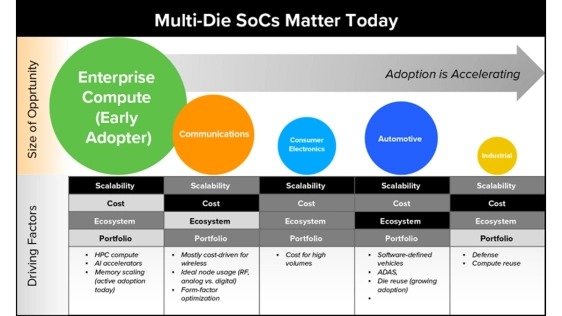
Across markets such as AI, high-performance computing (HPC), and automotive, the demand for computational power continues to accelerate. This demand spans everything from compact edge devices to massive data center servers. Traditionally, that capacity was delivered by monolithic systems-on-chip (SoCs) implemented on a single silicon die. While manufacturing trade-offs can ease some pressures, a large die still limits optimization, forcing designers to balance power and performance across the entire chip rather than fine-tuning each function individually.
 The problem is structural. Monolithic SoCs have reached physical and economic limits. Reticle size is fixed, yields decline as die size grows, and the cost of large devices is prohibitively high.
Multi-die systems offer a practical path forward. By breaking a large SoC into smaller chips, teams gain better yields, leverage proven components, and combine diverse process technologies in a single package. Additionally, chiplets can be reused across product lines, improving scalability and reducing cost.
The semiconductor industry has long envisioned chiplets as modular and interoperable, backed by fully proven standards. Companies are not waiting for that vision to materialize fully. They are already moving ahead with chiplet adoption while standards remain in flux.
Why chiplets, and why now?
To read the full article, click here
Related Chiplet
- eFPGA Chiplet
- DPIQ Tx PICs
- IMDD Tx PICs
- Near-Packaged Optics (NPO) Chiplet Solution
- High Performance Droplet
Related Blogs
- How Cadence Is Expanding Innovation for 3D-IC Design
- The Chiplet Center of Excellence sets new standards for the automotive industry
- Marvell Joins Imec Automotive Chiplet Initiative to Facilitate Compute SoCs for Super-human Sensing
- What is a Chiplet, and Why Should You Care?
Latest Blogs
- How Intel Foundry Packaging Technologies Redefine AI and HPC Scalability Limits at ECTC 2026
- From complexity to simplicity: Scaling and future-proofing chiplets with AMBA®︎ CHI C2C property negotiation
- High-Speed Heterogeneous Integration with Multiphysics Analysis for TSMC SoW-X
- Chiplet Realization Beyond the Package: Why the Next AI Bottleneck Moves to the Interposer-to-PCB Boundary
- Advancing UCIe Performance: Enabling 40G for Next-Generation Multi-Die Designs