Samsung Foundry Partners with Arm, ADTechnology and Rebellions to Develop an Innovative AI CPU Chiplet Platform Ideal for Modern AI Datacenters
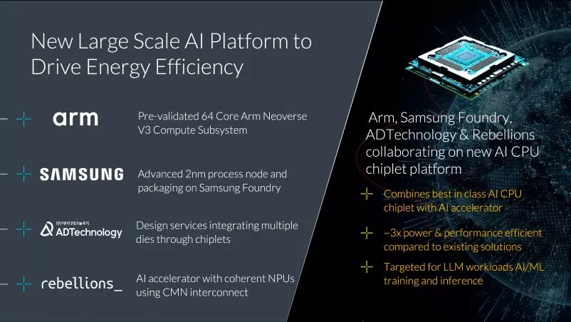
At the Open Compute Project (OCP) Global Summit 2024, Arm announced its collaboration with Samsung Foundry, ADTechnology, and Rebellions on an AI CPU chiplet platform for cloud, HPC, and AI/ML training and inference. Together, the partners will bring a new best-in-class AI CPU chiplet platform, built with Arm® Neoverse™ CSS V3 Compute Subsystems, Rebellions’ AI accelerator with NPUs using Arm CMN interconnect, Samsung Foundry’s 2nm Gate-All-Around (GAA) process node and advanced packaging, and ADTechnology’s end-to-end full turnkey design services. The multi-company collaboration aims to deliver an AI CPU chiplet platform with 2-3x efficiency advantage for GenAI workloads compared to other leading solutions (Llama3.1 405B parameter LLMs).
“Datacenters are under pressure to keep up with the fast-paced evolution of AI workloads and require new power efficient solutions that can meet the increasing need for greater performance,” said Eddie Ramirez, vice president of go-to-market, Infrastructure Line of Business, Arm. “Our collaboration with Samsung Foundry, ADTechnology and Rebellions is a terrific example of the unique value of Arm Total Design and standards-based compute subsystems in accelerating AI silicon development with significant efficiency gains.”

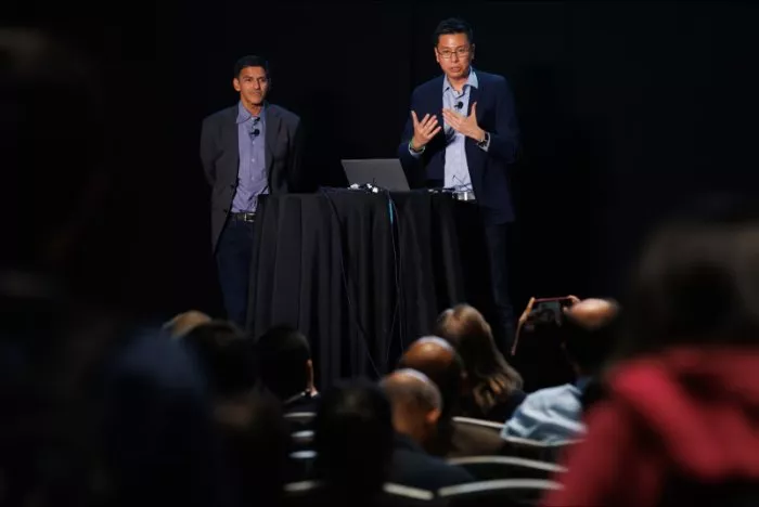
From left to right: Director Imran Yusuf at Arm & VP Kelvin Low at Samsung Foundry
At the OCP Summit, Kelvin Low, VP of market intelligence, business strategy and partnerships for US Samsung Foundry, and Imran Yusuf, director of hardware ecosystem, Infrastructure Line of Business at Arm, presented “Accelerating AI Innovation with Arm Total Design: A Case Study.” The report covered how their collaboration in the Arm Total Design ecosystem led to the development of an innovative AI chiplet platform for datacenters, networking, and telecom. The presentation explored key industry challenges and illustrated clear value propositions of the new AI CPU chiplet platform, including lower total development costs, faster time-to-market (TTM), and reduced risks from leveraging pre-validated solutions.

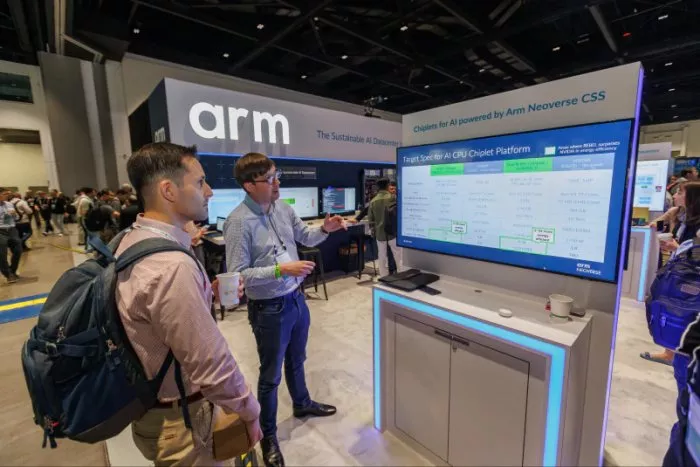
Thomas Mermans, senior director of business strategy at Samsung Foundry, is explaining the advantages of the four-way collaboration of Samsung Foundry, Arm, Rebellions, and ADTechnology
Samsung Foundry showcased its advanced 2nm process node and packaging solutions and demonstrated its technology collaboration on an AI CPU chiplet to the visitors at the Arm booth during OCP. Rebellions and ADTechnology were also there to showcase their innovative technologies as part of this collaboration.
“This four-way collaboration with Arm, Samsung Foundry, and ADTechnology aims to revolutionize AI infrastructure through a cutting-edge AI CPU chiplet platform. By integrating our REBEL AI accelerator, known for its scalability and high-bandwidth memory, with Arm's advanced compute subsystems and Samsung Foundry's 2nm process, we're creating a future-proof solution,” said Jinwook Oh, CTO of Rebellions. “This platform will deliver superior energy efficiency and performance for complex AI workloads in data centers and high-performance computing environments, enabling customers to tackle next-generation AI challenges more effectively.”
"Our collaboration with Samsung Foundry, Arm, and Rebellions marks a significant milestone in the development of a high-performance, energy-efficient AI CPU chiplet platform. ADTechnology will optimize the design of CPU clusters and interfaces to maximize performance and efficiency, securing a competitive edge and providing the best possible solutions," said JK Park, CEO of ADTechnology.

Overview of the four-way collaboration of the AI CPU chiplet platform
Samsung Semiconductor strives to lead the industry as a true comprehensive foundry service provider with leading-edge process technologies, advanced packaging, and IP ecosystem through SAFE™ (Samsung Advanced Foundry Ecosystem). As a technology leader, Samsung Foundry was first to production of 3nm nodes with GAA architecture. The next generation GAA at 2nm node incorporates additional enhancements optimized for HPC and AI applications. As part of a one-stop solution provider, Samsung Foundry works with Samsung Memory on industry-leading memory technologies including HBM3/4 and custom HBM base die, which is coupled with advanced packaging such as Samsung I-CubeS/R/E that enable a wide range of applications, supported by the broader SAFE Ecosystem of over 100 partners across EDA, IP, Design Solution Partners, Cloud and OSAT.
Related Chiplet
- DPIQ Tx PICs
- IMDD Tx PICs
- Near-Packaged Optics (NPO) Chiplet Solution
- High Performance Droplet
- Interconnect Chiplet
Related Blogs
- Inside the Chiplet Revolution: How Arm’s Compute Subsystems Platform is Democratizing Custom AI Silicon
- Intel® Shows OCI Optical I/O Chiplet Co-packaged with CPU at OFC2024, Targeting Explosive AI Scaling
- Cadence Recognized for Accelerating AI and 3D-IC Applications by Samsung Foundry
- Simplifying AI Chip Development: Arm and Synopsys Execs Discuss Chiplet, Subsystem, and IP Integration
Latest Blogs
- Chiplets: 8 best practices for engineering multi-die designs
- Demystifying 3D ICs: A practical framework for heterogeneous integration
- Accelerating Next-Generation EMIB-T Packaging: A Collaboration Between Synopsys and Intel Foundry
- Scoping out the chiplet-based design flow
- Understanding the Difference Between a Monolithic SoC and a Chiplet
