NHanced Semiconductors Opens Leading-Edge Advanced Package Assembly Facility, Reinforcing Indiana’s Position as a Major Semiconductor Hub
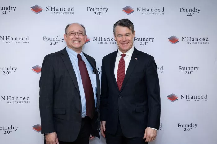
U.S. Senator Todd Young (R-IN) and NHanced Semiconductors President Robert Patti, at the ribbon-cutting at the Odon facility, announce new advanced semiconductor packaging capabilities, making the state a key player in Indiana’s high-tech future
ODON, IN -- JANUARY 22, 2024 – NHanced Semiconductors is a US-based pure-play advanced packaging foundry specializing in leading-edge technologies. NHanced president Robert Patti was joined by U.S. Senator Todd Young (R-IN); Andrea Richter-Garry, senior VP of the Indiana Economic Development Corporation (IEDC), representing Indiana Governor Eric Holcomb; and Dr. Kyle Werner, NSWC Crane Deputy Technical Director, at the ribbon-cutting ceremony for its NHanced WestGate Facility, a multimillion-dollar advanced package assembly center, on January 19. This represents the latest phase of a major investment program by NHanced to establish a world-class semiconductor and microelectronics ecosystem in Indiana.
Speaking at the NHanced WestGate Facility, Senator Young said, “Innovative companies like NHanced are not only providing good jobs, they are keeping us safe and secure by making technological advancements with military applications.” Senator Young continued, noting that the federal CHIPS and Science Act was passed, in part, to encourage investments like this: “Indiana is emerging as a key player in our high-tech future, and we’re grateful for the investment NHanced is making in Hoosiers.”
According to Patti, “This is our first step in bringing advanced semiconductor packaging to Indiana. Our final aim, when the WestGate One complex is complete, is to deliver full Foundry 2.0 services to fulfill the needs of the US Government.”
Representing Governor Holcomb’s office, Andrea Richter-Garry, Senior Vice President of Global Strategy and Engagement at the Indiana Economic Development Corporation said, “Indiana is taking bold action to put our state at the forefront of critical innovations and key industries in order to create a more prosperous future for Hoosiers.” She added, “We’ve become a destination of choice for the semiconductor industry. Our state offers a robust tech ecosystem to support semiconductor manufacturing and development throughout all levels of the microelectronics value chain.”
“NSWC Crane is delighted to help kick off the important semiconductor packaging work that will happen at NHanced and the WestGate One complex,” said Dr. Kyle Werner, NSWC Crane Deputy Technical Director. “Advanced semiconductor technology is central to supporting our nation’s Nuclear Triad and priority nuclear modernization efforts underway. Working with NHanced, and so many others, the Innovation Ecosystem at NSWC Crane accelerates the development of critical solutions to advance Warfighter capabilities that keep our nation safe. A special thank you to all partners involved and NSWC Crane very much looks forward for what’s to come,” he said.
The new Odon NHanced facility features two state-of-the art cleanrooms - one will house the company’s semiconductor advanced package assembly line and the other is planned for process development and training, specifically for the NHanced foundry in Bloomington, expected to open later this year.
The Odon facility is designed as part of WestGate One - a multi-company complex that will be the first semiconductor foundry in the US built specifically for advanced package manufacturing. NHanced and several other semiconductor companies will occupy the ten-acre public-private development adjacent to the Crane Naval Surface Warfare Center, with future partnerships expected with industry, government, and educational institutions.
The combined companies of WestGate One are expected to create more than 500 high-tech jobs with average salaries of more than $100K/year.
Both the companies and the governments have announced commitments to support training initiatives for the new workforce. NHanced is already working with Indiana universities and trade schools to build the workforce; future plans include STEM efforts for K-12 education.

Photo caption: (left to right) NHanced Semiconductors President Robert Patti & U.S. Senator Todd Young (R-IN)
About NHanced Semiconductors, Inc.
NHanced Semiconductors is the first pure-play advanced packaging foundry in the US, specializing in leading-edge BEoL semiconductor technologies including chiplets, 3D-ICs, silicon interposers, 2.5D, additive silicon manufacturing, photonics, microfluidics, and other innovative technologies. The foundry works with both standard and non-standard substrates, III‑V compound semiconductors, and many specialized materials.
Headquartered in Illinois, NHanced also has a development and manufacturing facility near Research Triangle Park, NC, performing small volume manufacturing, in-house process development, and customer prototyping.
About NSWC Crane
NSWC Crane is a naval laboratory and a field activity of Naval Sea Systems Command (NAVSEA) with mission areas in Expeditionary Warfare, Strategic Missions, and Electromagnetic Warfare. The warfare center is responsible for multi-domain, multi- spectral, full life cycle support of technologies and systems enhancing capability to today's Warfighter.
Related Chiplet
- DPIQ Tx PICs
- IMDD Tx PICs
- Near-Packaged Optics (NPO) Chiplet Solution
- High Performance Droplet
- Interconnect Chiplet
Related News
- NHanced Semiconductors to Commission Advanced Package Assembly Facility In Indiana
- NHanced Semiconductors Announces Delivery of the First Next-Generation Hybrid Bonding System from BE Semiconductor Industries
- NHanced Semiconductors Leads the Semiconductor Industry in Heterogeneous Hybrid Bonding Production
- Athos Silicon Selects DreamBig Semiconductor’s Chiplet Hub™ for its Safety-Critical mSoC™ Platform Designed Ground-up for Autonomy
Latest News
- CEA-Leti, CEA-List and PSMC Collaborate to Integrate RISC-V and MicroLED Silicon Photonics into 3D Stacking and Interposer for Next-Generation AI
- NIST Researchers Develop Photonic Chip Packaging That Can Withstand Extreme Environments
- Rebellions Closes $400 Million Pre-IPO and Launches RebelRack™ and RebelPOD™ to Accelerate Global Expansion
- EdgeCortix Looks To Chiplets For Third-Gen Reconfigurable AI Chip
- Agileo Automation Launches Agil'EDA to Accelerate SEMI EDA Adoption for Semiconductor Equipment OEMs