CEA-Leti & STMicroelectronics’ Paper at IEDM 2025 Demonstrates Path to Fully Monolithic Silicon RF Front-Ends with 3D Sequential Integration
Joint Work Shows Next Generations of RF and Optical Front-End Modules (FEM) Could Be Built by the Assembly of Different Silicon Technologies at Wafer Level, Allowing the Dense Co-integration of Best-In Class Functions.
SAN FRANCISCO — Dec. 11, 2025 — CEA-Leti and STMicroelectronics today presented results at IEDM 2025 showcasing key enablers for a new high-performance and versatile RF Si platform cointegrating best-in-class active and passive devices used in RF and Optical FEM. Their paper details 3D sequential integration of silicon-germanium (SiGe) heterojunction bipolar transistors (HBT), RF SOI switches, and high-quality passives on a single wafer—opening a path to highly integrated, low parasitic, and targeting cost-efficient systems for next-generation wireless and wireline communications.
The paper, “Unlocking High-Performance Si RF Platforms with SiGe HBT and RFSOI Switch Technologies,” describes how those high-performance components can be built directly on the same silicon wafer rather than packaged or stacked as separate chips. This can be achieved through 3D sequential integration, which layers different device types, such as SiGe HBT and SOI CMOS switches, without overheating the lower tiers during processing.
‘Efficient and Cost-Effective’
“Our team has shown that high-performance SiGe HBT has been conceived to be compatible with the top-tier fabrication steps, and that trap-rich isolation can be localized and thermally robust, and low-temperature (600°C) SOI switches can match state-of-the-art figures of merits,” said CEA-Leti’s Thibaud Fache, lead author of the paper. “These results pave the way to an all-silicon RF front-end module that is efficient and cost-effective.”
The team showed that a localized trap rich layer can achieve RF isolation and linearity comparable to costly commercial trap-rich substrates, while withstanding thermal cycles up to 600 °C—preserving the performance of the underlying SiGe HBT layer.
‘From Advanced Research to Manufacturable Solutions’
By extending silicon’s reach of sequential integration into the RF domain, the CEA-Leti/ST team’s work points to a future of more accessible, energy-efficient connectivity. Fully integrated RF and optical front ends could simplify the manufacturing and enable cost-effective deployment of dense wireless networks essential for smart cities, autonomous systems, and AI datacenters.
“This joint result demonstrates a credible path from advanced research to manufacturable solutions,” said ST’s Thomas Bordignon, co-author of the paper. “By combining CEA-Leti’s sequential integration know-how with ST’s RF technology expertise, we’re enabling the co-integration of state-of-the-art SiGe HBT, switches and passive devices, that are key elements of the FEM.”
Materials Science Milestone
Achieving a performant RF Partially Depleted (PD) SOI switch at 600 °C rather than standard ~1000 °C is a first. It is worth noting that process flow of this low-temperature device does not rely on new equipment or costly steps and is thus quickly industrially viable thanks to the relatively relaxed thermal budget constraints of bottom tier (600°C). The team demonstrated high-quality, low-loss RF switches fabricated at 600 °C, maintaining the performance of the SiGe HBT below and confirming the feasibility of a fully integrated silicon RF platform.
Additional Breakthrough Presentation
CEA-Leti researchers will report tomorrow a major breakthrough (session 33-4) with the design of high-performance silicon-on-insulator (SOI) MOSFETs processed at 400°C. NMOS and pMOS transistors demonstrate state-of-the art performances among the Back-End-Of-Line devices, fulfilling all industrial figures of merit without any compromise. This reliable versatile analog transistor targets More Than Moore applications bringing differential advantage for smart sensors, near memory computing and RF devices. More details in “33-4 | High Performance 2.5V N&P 400°C SOI MOSFETs: A Breakthrough for Versatile 3D Sequential Integration”.
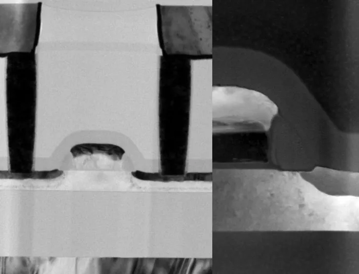
TEM cross section of 600°C RF switch processed on standard TR commercial wafer
Photo credit: Julie LOCHE/STMicroelectronics
About CEA-Leti (France)
CEA-Leti, a technology research institute at CEA, is a global leader in miniaturization technologies enabling smart, energy-efficient and secure solutions for industry. Founded in 1967, CEA-Leti pioneers micro-& nanotechnologies, tailoring differentiating applicative solutions for global companies, SMEs and startups. CEA-Leti tackles critical challenges in healthcare, energy and digital migration. From sensors to data processing and computing solutions, CEA-Leti’s multidisciplinary teams deliver solid expertise, leveraging world-class pre-industrialization facilities. With a staff of more than 2,000 talents, a portfolio of 3,200 patents, 11,000 sq. meters of cleanroom space and a clear IP policy, the institute is based in Grenoble (France) and has offices in San Francisco (United States), Brussels (Belgium), Tokyo (Japan), Seoul (South Korea) and Taipei (Taiwan). CEA-Leti has launched 80 startups and is a member of the Carnot Institutes network. Follow us on www.leti-cea.com and @CEA_Leti.
Technological expertise
CEA has a key role in transferring scientific knowledge and innovation from research to industry. This high-level technological research is carried out in particular in electronic and integrated systems, from microscale to nanoscale. It has a wide range of industrial applications in the fields of transport, health, safety and telecommunications, contributing to the creation of high-quality and competitive products.
For more information: www.cea.fr/english
Related Chiplet
- DPIQ Tx PICs
- IMDD Tx PICs
- Near-Packaged Optics (NPO) Chiplet Solution
- High Performance Droplet
- Interconnect Chiplet
Related News
- Imec achieves seamless InP Chiplet integration on 300mm RF Silicon Interposer with excellent performance at 140GHz
- 300mm RF silicon interposer platform for chiplet-based heterogeneous integration demonstrates record-low insertion loss at frequencies up to 325GHz
- Scintil Photonics, Presto Engineering and CEA-Leti Receive Bpifrance Grant for the CanopAI Project to Advance Photonic Integration for AI and Data Centers
- Veeco and imec develop 300mm compatible process to enable integration of barium titanate on silicon photonics
Latest News
- NIST Researchers Develop Photonic Chip Packaging That Can Withstand Extreme Environments
- Rebellions Closes $400 Million Pre-IPO and Launches RebelRack™ and RebelPOD™ to Accelerate Global Expansion
- EdgeCortix Looks To Chiplets For Third-Gen Reconfigurable AI Chip
- Agileo Automation Launches Agil'EDA to Accelerate SEMI EDA Adoption for Semiconductor Equipment OEMs
- AEM and ASE Enter Strategic Partnership to Accelerate AI and HPC Test Innovation